MOTOROLA MMVL105GT1 Datasheet

MMVL105GT1
Preferred Device
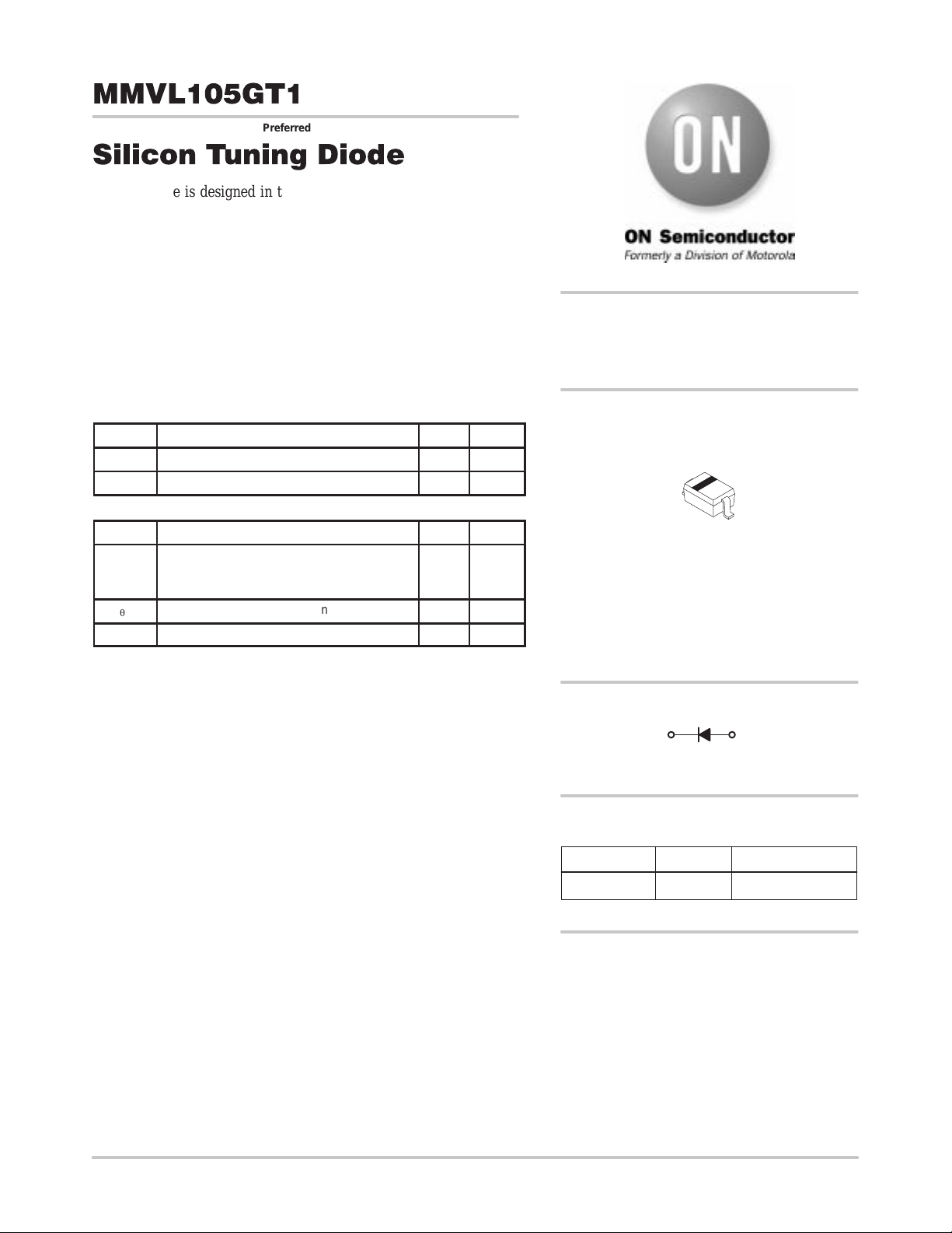
Silicon Tuning Diode
This device is designed in the Surface Mount package for general
frequency control and tuning applications. It provides solid–state
reliability in replacement of mechanical tuning methods.
• Controlled and Uniform Tuning Ratio
• Device Marking: 4E
MAXIMUM RATINGS
Symbol Rating Value Unit
V
I
THERMAL CHARACTERISTICS
Symbol Characteristic Max Unit
P
R
q
TJ, T
*FR–4 Minimum Pad
Continuous Reverse Voltage 30 Vdc
R
Peak Forward Current 200 mAdc
F
Total Device Dissipation FR–5 Board,*
D
JA
stg
T
= 25°C
A
Derate above 25°C
Thermal Resistance Junction to Ambient 635 °C/W
Junction and Storage Temperature 150 °C
200
1.57mWmW/°C
http://onsemi.com
30 VOLT
VOLTAGE VARIABLE
CAPACITANCE DIODE
1
2
PLASTIC
SOD–323
CASE 477
Semiconductor Components Industries, LLC, 2000
January , 2000 – Rev. 1
1
CATHODE
2
ANODE
ORDERING INFORMATION
Device Package Shipping
MMVL105GT1 SOD–323 3000 / Tape & Reel
Preferred devices are recommended choices for future use
and best overall value.
1 Publication Order Number:
MMVL105GT1/D

MMVL105GT1
ELECTRICAL CHARACTERISTICS (T
Characteristic
Reverse Breakdown Voltage
(I
= 10 µAdc)
R
Reverse Voltage Leakage Current
(V
= 28 Vdc)
R
Device Type
= 25°C unless otherwise noted)
A
Symbol Min Typ Max Unit
C
T
VR = 25 Vdc, f = 1.0 MHz
pF
V
(BR)R
I
R
Q
= 3.0 Vdc
V
R
f = 50 MHz
30 — Vdc
— 50 nAdc
C
R
C3/C
25
f = 1.0 MHz
Min Max Typ Min Max
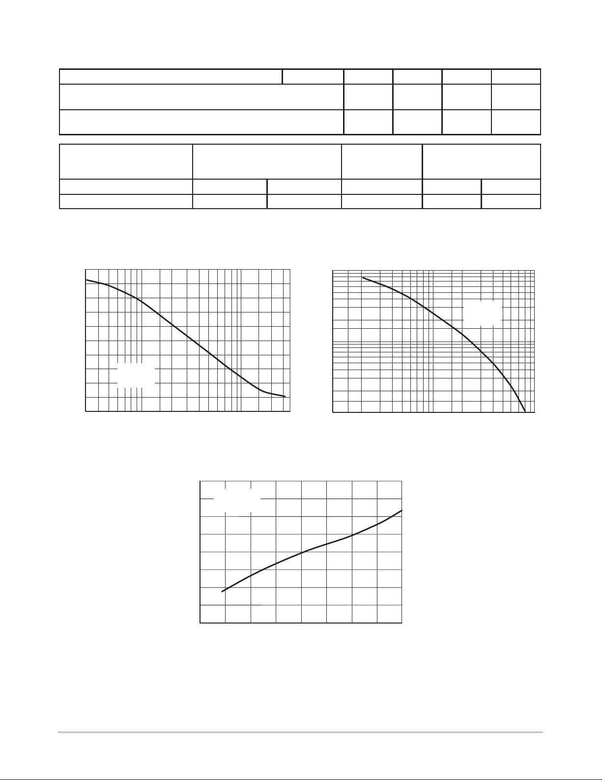
MMVL105GT1 1.5 2.8 250 4.0 6.5
TYPICAL CHARACTERISTICS
20
18
16
14
12
10
8.0
, DIODE CAPACITANCE (pF)
T
C
6.0
4.0
f = 1.0 MHz
T
= 25°C
A
2.0
0
0.3 1.0 10 20 30
0.5 2.0 3.0 5.0
V
, REVERSE VOLTAGE (VOLTS)
R
1000
100
Q, FIGURE OF MERIT
10
10
VR = 3 Vdc
T
A
100 1000
f, FREQUENCY (MHz)
= 25°C
Figure 1. Diode Capacitance
1.04
1.03
1.02
1.01
1.00
0.99
0.98
, DIODE CAPACITANCE (NORMALIZED)
0.97
T
C
0.96
VR = 3.0 Vdc
f = 1.0 MHz
–75
–50 0 +50 +100
Figure 2. Figure of Merit
–25 +25 +75 +125
TA, AMBIENT TEMPERATURE (°C)
Figure 3. Diode Capacitance
http://onsemi.com
2
 Loading...