

MOTOROLA MMSF5P02HD Technical data
S5P02H
查询MMSF5P02HD/D供应商
SEMICONDUCTOR TECHNICAL DATA
Order this document
by MMSF5P02HD/D
Medium Power Surface Mount Products
MiniMOS devices are an advanced series of power MOSFETs
which utilize Motorola’s High Cell Density HDTMOS process. These
miniature surface mount MOSFETs feature ultra low R
logic level performance. They are capable of withstanding high energy in
the avalanche and commutation modes and the drain–to–s ource diode
has a very low reverse recovery time. MiniMOS devices are designed for
use in low voltage, high speed switching applications where power
efficiency is important. Typical applications are dc–dc converters, and
power management in portable and battery powered products such as
computers, printers, cellular and cordless phones. They can also be
used for low voltage motor controls in mass storage products such as
disk drives and tape drives. The avalanche energy is specified to
eliminate the guesswork in designs where induc tive loads are switched
and offer additional safety margin against unexpected voltage transients.
• Ultra Low R
• Logic Level Gate Drive — Can Be Driven by Logic ICs
• Miniature SO–8 Surface Mount Package — Saves Board Space
• Diode Is Characterized for Use In Bridge Circuits
• Diode Exhibits High Speed, With Soft Recovery
• I
• Avalanche Energy Specified
• Mounting Information for SO–8 Package Provided
Specified at Elevated Temperature
DSS
Provides Higher Efficiency and Extends Battery Life
DS(on)
DS(on)
and true
Motorola Preferred Device
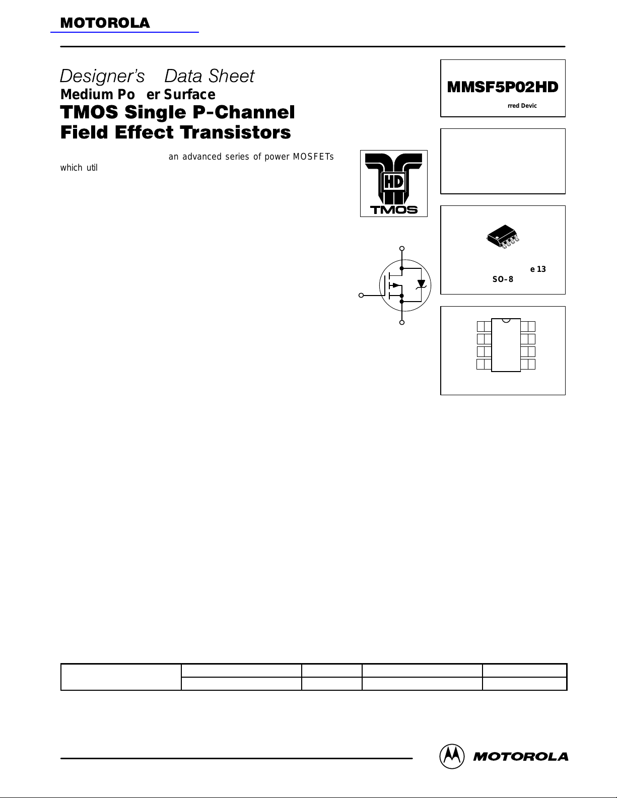
SINGLE TMOS
POWER MOSFET
8.7 AMPERES
20 VOLTS
R
D
CASE 751–05, Style 13
G
S
Source
Source
Source
Gate
DS(on)
= 0.03 OHM
SO–8
1
8
2
7
3
6
4
5
Top View
Drain
Drain
Drain
Drain
DEVICE MARKING ORDERING INFORMATION
Device Reel Size Tape Width Quantity
MMSF5P02HDR2 13″ 12 mm embossed tape 4000 units
Designer’s Data for “Worst Case” Conditions — The Designer’s Data Sheet permits the design of most circuits entirely from the information presented. SOA Limit
curves — representing boundaries on device characteristics — are given to facilitate “worst case” design.
HDTMOS and MiniMOS are trademarks of Motorola, Inc. TMOS is a registered trademark of Motorola, Inc.
Preferred devices are Motorola recommended choices for future use and best overall value.
REV 2
Motorola TMOS Power MOSFET Transistor Device Data
Motorola, Inc. 1997
1
MMSF5P02HD
MAXIMUM RATINGS
Negative sign for P–Channel devices omitted for clarity
Drain–to–Source Voltage V
Drain–to–Gate Voltage (RGS = 1.0 MΩ) V
Gate–to–Source Voltage — Continuous V
1 inch SQ.
FR–4 or G–10 PCB
10 seconds
Minimum
FR–4 or G–10 PCB
10 seconds
Operating and Storage Temperature Range TJ, T
Single Pulse Drain–to–Source Avalanche Energy — Starting TJ = 25°C
(VDD = 20 Vdc, VGS = 4.5 Vdc, Peak IL = 19 Apk, L = 5.5 mH, RG = 25 W)
(1) Repetitive rating; pulse width limited by maximum junction temperature.
(TJ = 25°C unless otherwise noted)
Rating
Thermal Resistance — Junction to Ambient
Total Power Dissipation @ TA = 25°C
Linear Derating Factor
Drain Current — Continuous @ TA = 25°C
Continuous @ TA = 70°C
Pulsed Drain Current
Thermal Resistance — Junction to Ambient
Total Power Dissipation @ TA = 25°C
Linear Derating Factor
Drain Current — Continuous @ TA = 25°C
Continuous @ TA = 70°C
Pulsed Drain Current
(1)
(1)
Symbol Max Unit
20 V
20 V
± 8.0 V
50
2.5
20
8.7
7.0
43.5
80
1.56
12.5
6.9
5.5
35
– 55 to 150 °C
1000
°C/W
Watts
mW/°C
°C/W
Watts
mW/°C
mJ
A
A
A
A
A
A
R
THJA
I
R
THJA
I
E
DSS
DGR
GS
P
D
I
D
I
D
DM
P
D
I
D
I
D
DM
stg
AS
2
Motorola TMOS Power MOSFET Transistor Device Data
MMSF5P02HD
)
f = 1.0 MHz)
V
G
)( )
(
DS
,
D
,
(
S
,
GS
,
ELECTRICAL CHARACTERISTICS (T
Characteristic Symbol Min Typ Max Unit
OFF CHARACTERISTICS
Drain–to–Source Breakdown Voltage (Cpk ≥ 2.0) (1) (3)
(VGS = 0 Vdc, ID = 0.25 mAdc)
T emperature Coef ficient (Positive)
Zero Gate Voltage Drain Current
(VDS = 16 Vdc, VGS = 0 Vdc)
(VDS = 16 Vdc, VGS = 0 Vdc, TJ = 125°C)
Gate–Body Leakage Current (VGS = ± 8.0 Vdc, VDS = 0) I
(1)
(1)
Cpk =
(2)
Max limit – Typ
ON CHARACTERISTICS
Gate Threshold Voltage (Cpk ≥ 2.0) (1) (3)
(VDS = VGS, ID = 0.25 mAdc)
Threshold Temperature Coefficient (Negative)
Static Drain–to–Source On–Resistance (Cpk ≥ 2.0) (1) (3)
(VGS = 4.5 Vdc, ID = 6.4 Adc)
(VGS = 2.5 Vdc, ID = 5.1 Adc)
On–State Drain Current
(VDS ≤ 5.0 V, VGS = 4.5 V)
(VDS ≤ 5.0 V, VGS = 2.5 V)
Forward Transconductance (VDS = 9.0 Vdc, ID = 6.4 Adc) (1) g
DYNAMIC CHARACTERISTICS
Input Capacitance
Output Capacitance
Transfer Capacitance
SWITCHING CHARACTERISTICS
Turn–On Delay Time
Rise Time
Turn–Off Delay Time
Fall Time
Gate Charge
See Figure 8
SOURCE–DRAIN DIODE CHARACTERISTICS
Forward On–Voltage
Reverse Recovery Time
See Figure 15
Reverse Recovery Stored Charge Q
(1) Pulse Test: Pulse Width ≤ 300 µs, Duty Cycle ≤ 2%.
(2) Switching characteristics are independent of operating junction temperature.
(3) Reflects typical values.
(4) Repetitive rating; pulse width limited by maximum junction temperature.
= 25°C unless otherwise noted)
C
(VDS = 16 Vdc, VGS = 0 Vdc,
(VDD = 6.0 Vdc, ID = 1.0 Adc,
(VDS = 6.0 Vdc, ID = 6.4 Adc,
(IS = 2.5 Adc, VGS = 0 Vdc) (1)
(IS = 2.5 Adc, VGS = 0 Vdc, TJ = 125°C)
3 x SIGMA
f = 1.0 MHz
= 4.5 Vdc,
GS
RG = 6.0 Ω) (1)
VGS = 4.5 Vdc) (1)
(IS = 2.5 Adc, VGS = 0 Vdc,
dIS/dt = 100 A/µs) (1)
V
(BR)DSS
I
DSS
GSS
V
GS(th)
R
DS(on)
I
D(on)
FS
C
iss
C
oss
C
rss
t
d(on)
t
r
t
d(off)
t
f
Q
Q
Q
Q
V
SD
t
rr
t
a
t
b
RR
20
—
—
—
— — 100 nAdc
0.7
—
—
—
10
5.0
14 18 — Mhos
— 1400 1960 pF
— 925 1300
— 370 520
— 19 40
— 28 55
— 130 200
— 90 150
T
1
2
3
— 27.3 38
— 3.4 —
— 12 —
— 8.0 —
—
—
— 95 180
— 35 —
— 60 —
— 0.151 — µC
—
10
—
—
0.9
2.6
22
35
—
—
0.77
0.6
—
—
1.0
25
1.4
—
30
45
—
—
1.2
—
Vdc
mV/°C
µAdc
Vdc
mV/°C
mΩ
A
ns
nC
Vdc
ns
Motorola TMOS Power MOSFET Transistor Device Data
3
MMSF5P02HD
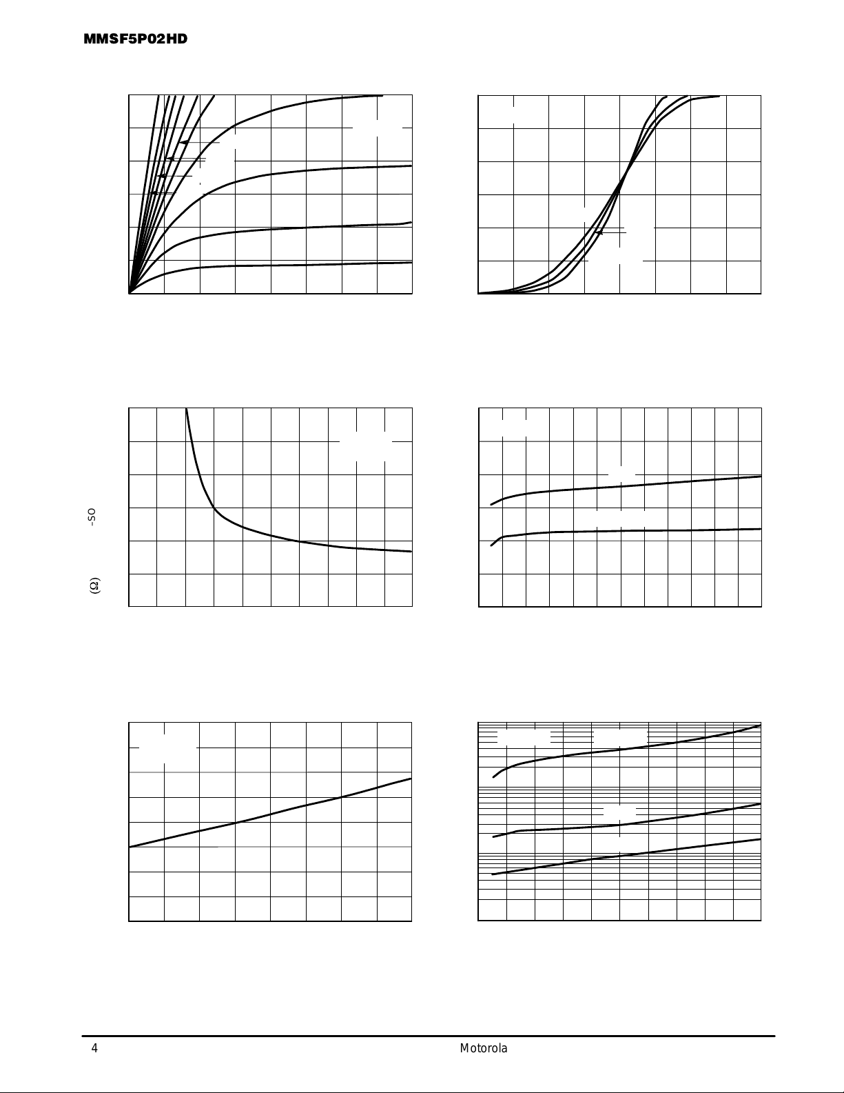
TYPICAL ELECTRICAL CHARACTERISTICS
12
10
8.0
6.0
4.0
, DRAIN CURRENT (AMPS)
D
I
2.0
0
0.06
0.04
VGS =
8
2.5 V
2.7 V
3.1 V
3.7 V
4.5 V
0.5 1.0 1.5 2.51.5 2.0
VDS, DRAIN–TO–SOURCE VOL TAGE (VOLTS)
2.3 V
TJ = 25°C
2.1 V
1.9 V
1.7 V
2.00
12
VDS ≥ 10 V
10
8.0
6.0
4.0
D
I
2.0
0
VGS, GATE–T O–SOURCE VOLT AGE (VOLTS)
100°C
25°C
TJ = –55°C
Figure 1. On–Region Characteristics Figure 2. Transfer Characteristics
0.06
ID = 6.4 A
TJ = 25
°
C
0.04
TJ = 25°C
2.5 V
3.01.0
VGS = 4.5 V
0.02
, DRAIN–TO–SOURCE RESIST ANCE (OHMS)
(W)
0
DS(on)
R
0
2.0 4.0 6.0 8.0 10 6.0 8.0
VGS, GATE–T O–SOURCE (VOLTS)
0.02
, DRAIN–TO–SOURCE RESIST ANCE (OHMS)
0
DS(on)
R
2.00
4.0
ID, DRAIN CURRENT (AMPS)
Figure 3. On–Resistance versus Drain Current Figure 4. On–Resistance versus Drain Current
and Gate Voltage
2.0
VGS = 4.5 V
ID = 5.1 A
1.5
1.0
(NORMALIZED)
0.5
, DRAIN–TO–SOURCE RESIST ANCER
DS(on)
0
–25 25–50
TJ, JUNCTION TEMPERATURE (
50 10075 8.0 12 20
°
C)
125 150
1000
100
, LEAKAGE (nA) , DRAIN CURRENT (AMPS)
10
DSS
I
1.0
VGS = 0 V
4.00
VDS, DRAIN–TO–SOURCE VOL TAGE (VOLTS)
TJ = 125°C
100°C
25°C
10 12
160
Figure 5. On–Resistance Variation with
T emperature
4
Figure 6. Drain–to–Source Leakage Current
versus V oltage
Motorola TMOS Power MOSFET Transistor Device Data
 Loading...