

MOTOROLA MMSD914T1 Technical data
查询MMSD914T1/D供应商
SEMICONDUCTOR TECHNICAL DATA
The switching diode has the following features:
• SOD–123 Surface Mount Package
• High Breakdown Voltage
• Fast Speed Switching Time
Order this document
by MMSD914T1/D
Motorola Preferred Device
1
Cathode
MAXIMUM RATINGS
Rating Symbol Value Unit
Continuous Reverse Voltage V
Peak Forward Current I
Peak Forward Surge Current I
DEVICE MARKING
MMSD914T1 = 5D
THERMAL CHARACTERISTICS
Characteristic Symbol Max Unit
Total Device Dissipation FR–5 Board
TA = 25°C
Derate above 25°C
Thermal Resistance Junction to Ambient
Total Device Dissipation
Alumina Substrate
Derate above 25°C
Thermal Resistance Junction to Ambient
Junction and Storage Temperature TJ, T
(2)
TA = 25°C
ELECTRICAL CHARACTERISTICS (T
Characteristic Symbol Min Max Unit
(1)
= 25°C unless otherwise noted)
A
OFF CHARACTERISTICS
Reverse Breakdown Voltage (IBR = 100 µAdc) V
Reverse Voltage Leakage Current (VR = 20 Vdc)
Forward Voltage (IF = 10 mAdc) V
Diode Capacitance (VR = 0 Vdc, f = 1.0 MHz) C
Reverse Recovery Time (IF = IR = 10 mAdc) (Figure 1) t
1. FR–5 = 1.0 x 0.75 x 0.062 in.
2. Alumina = 0.4 x 0.3 x 0.024 in. 99.5% alumina
(VR = 75 Vdc)
R
F
FM(surge)
P
D
R
q
JA
P
D
R
q
JA
stg
(BR)
I
R
F
D
rr
2
Anode
1
CASE 425–04, STYLE 1
SOD–123
100 Vdc
200 mAdc
500 mAdc
225
1.8
556 °C/W
300
2.4
417 °C/W
–55 to +150 °C
100 — Vdc
—
—
— 1000 mVdc
— 4.0 pF
— 4.0 ns
25
5.0
2
mW
mW/°C
mW
mW/°C
nAdc
m
Adc
Preferred devices are Motorola recommended choices for future use and best overall value.
Thermal Clad is a registered trademark of the Berquist Company .
REV 2
Motorola Small–Signal Transistors, FETs and Diodes Device Data
Motorola, Inc. 1997
1
MMSD914T1
820
Ω
+10 V
0.1 µF
2 k
100
0.1
µ
I
F
µ
H
F
t
t
r
p
10%
t
I
F
t
rr
t
Ω
OUTPUT
50
PULSE
GENERATOR
100
10
TA = 85
1.0
, FORWARD CURRENT (mA)
F
I
DUT
50 Ω INPUT
SAMPLING
OSCILLOSCOPE
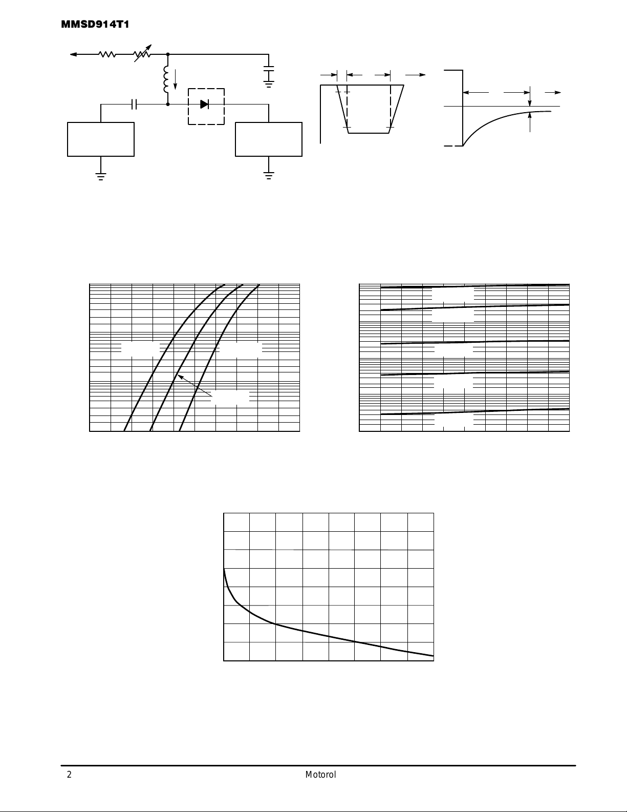
Notes: 1. A 2.0 kΩ variable resistor adjusted for a Forward Current (IF) of 10 mA.
Notes: 2. Input pulse is adjusted so I
Notes: 3. tp » t
rr
V
R(peak)
R
90%
INPUT SIGNAL
is equal to 10 mA.
Figure 1. Recovery Time Equivalent Test Circuit
10
µ
1.0
°
C
TA = –40°C
TA = 25°C
, REVERSE CURRENT ( A)
R
I
0.1
0.01
I
R
TA = 150°C
TA = 125°C
TA = 85°C
TA = 55°C
i
= 1 mA
R(REC)
OUTPUT PULSE
(IF = IR = 10 mA; measured
at i
R(REC)
= 1 mA)
0.1
0.2 0.4
TA = 25°C
0.6 0.8 1.0
VF, FORWARD VOLTAGE (VOLTS)
1.2
0.001
0
10 20 30 40 50
VR, REVERSE VOLTAGE (VOLTS)
Figure 2. Forward V oltage Figure 3. Leakage Current
0.68
0.64
0.60
, DIODE CAPACITANCE (pF)
0.56
D
C
0.52
0
2468
VR, REVERSE VOLTAGE (VOLTS)
Figure 4. Capacitance
2
Motorola Small–Signal Transistors, FETs and Diodes Device Data
 Loading...