

Motorola MJW16010A Datasheet
1
Motorola Bipolar Power Transistor Device Data
1 kV SWITCHMODE Series
These transistors are designed for high–voltage, high–speed, power switching in
inductive circuits where fall time is critical. T hey a re particularly s uited f or
line–operated switchmode applications.
Typical Applications: Features:
• Switching Regulators • Collector–Emitter Voltage — V
CEV
= 1000 Vdc
• Inverters • Fast Turn–Off Times
• Solenoids 50 ns Inductive Fall Time — 100_C (Typ)
• Relay Drivers 90 ns Inductive Crossover Time — 100_C (Typ)
• Motor Controls 900 ns Inductive Storage Time — 100_C (Typ)
• Deflection Circuits • 100_C Performance Specified for:
Reverse–Biased SOA with Inductive Load
Switching Times with Inductive Loads
Saturation Voltages
Leakage Currents
• Extended FBSOA Rating Using Ultra–fast Rectifiers
• Extremely High RBSOA Capability
MAXIMUM RATINGS
Rating
Symbol
Value
Unit
Collector–Emitter Voltage
V
CEO
500
Vdc
Collector–Emitter Voltage
V
CEV
1000
Vdc
Emitter–Base Voltage
V
EB
6
Vdc
Collector Current—
Continuous
— Peak
(1)
I
C
I
CM
15
20
Adc
Base Current — Continuous
— Peak
(1)
I
B
I
BM
10
15
Adc
Total Power Dissipation
@ TC = 25_C
@ TC = 100_C
Derate above TC = 25_C
P
D
135
54
1.09
Watts
W/_C
Operating and Storage Junction
Temperature Range
TJ, T
stg
–55 to 150
I
C
THERMAL CHARACTERISTICS
Characteristic
Symbol
Max
Unit
Thermal Resistance, Junction to Case
R
θJC
0.92
_
C/W
Lead Temperature for Soldering Purposes:
1/8″ from Case for 5 Seconds
T
L
275
_
C
(1) Pulse Test: Pulse Width = 5 ms, Duty Cyclev 10%.
Designer’s Data for “Worst Case” Conditions — The Designer’s Data Sheet permits the design of most circuits entirely from the information presented. SOA Limit
curves — representing boundaries on device characteristics — are given to facilitate “worst case” design.
Preferred devices are Motorola recommended choices for future use and best overall value.
Designer’s and SWITCHMODE are trademarks of Motorola, Inc.
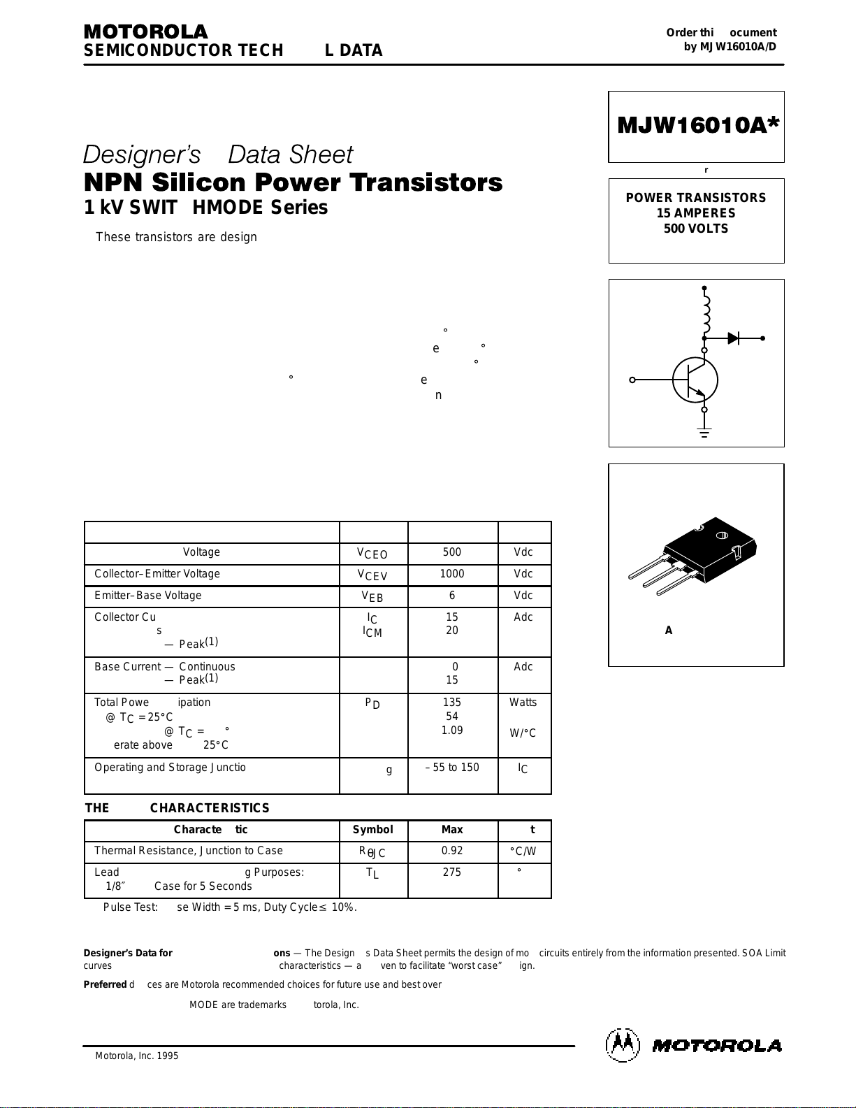
SEMICONDUCTOR TECHNICAL DATA
Order this document
by MJW16010A/D
Motorola, Inc. 1995
POWER TRANSISTORS
15 AMPERES
500 VOLTS
125 AND 175 WATTS
*Motorola Preferred Device
CASE 340F–03
TO–247AE
REV 3
MJW16010A
2
Motorola Bipolar Power Transistor Device Data
ELECTRICAL CHARACTERISTICS (T
C
= 25_C unless otherwise noted)
Characteristic
Symbol
Min
Typ
Max
ÎÎÎ
ÎÎÎ
ÎÎÎ
Unit
OFF CHARACTERISTICS
(1)
Collector–Emitter Sustaining Voltage (Table 1)
(IC = 100 mA, IB = 0)
V
CEO(sus)
500
—
—
ÎÎÎ
ÎÎÎ
ÎÎÎ
ÎÎÎ
Vdc
Collector Cutoff Current
(V
CEV
= 1000 Vdc, V
BE(off)
= 1.5 Vdc)
(V
CEV
= 1000 Vdc, V
BE(off)
= 1.5 Vdc, TC = 100_C)
I
CEV
—
—
0.003
0.020
0.15
1.0
ÎÎÎ
ÎÎÎ
ÎÎÎ
ÎÎÎ
mAdc
Collector Cutoff Current
(VCE = 1000 Vdc, RBE = 50 Ω, TC = 100_C)
I
CER
—
0.020
1.0
ÎÎÎ
ÎÎÎ
ÎÎÎ
ÎÎÎ
mAdc
Emitter Cutoff Current
(VEB = 6 Vdc, IC = 0)
I
EBO
—
0.005
0.15
ÎÎÎ
ÎÎÎ
ÎÎÎ
ÎÎÎ
mAdc
SECOND BREAKDOWN
Second Breakdown Collector Current with Base Forward Biased
I
S/b
See Figure 14a or 14b
Clamped Inductive SOA with Base Reverse Biased
RBSOA
See Figure 15
ON CHARACTERISTICS
(1)
Collector–Emitter Saturation Voltage
(IC = 5 Adc, IB = 1 Adc)
(IC = 10 Adc, IB = 2 Adc)
(IC = 10 Adc, IB = 2 Adc, TC = 100_C)
V
CE(sat)
—
—
—
0.25
0.45
0.60
0.7
1
1.5
ÎÎÎ
ÎÎÎ
ÎÎÎ
ÎÎÎ
ÎÎÎ
Vdc
Base–Emitter Saturation Voltage
(IC = 10 Adc, IB = 2 Adc)
(IC = 10 Adc, IB = 2 Adc, TC = 100_C)
V
BE(sat)
—
—
1.2
1.2
1.5
1.5
ÎÎÎ
ÎÎÎ
ÎÎÎ
ÎÎÎ
Vdc
DC Current Gain
(IC = 15 Adc, VCE = 5 Vdc)
h
FE
5
8
—
ÎÎÎ
ÎÎÎ
ÎÎÎ
ÎÎÎ
—
DYNAMIC CHARACTERISTICS
Output Capacitance
(VCB = 10 Vdc, IE = 0, f
test
= 1 kHz)
C
ob
—
—
400
ÎÎÎ
ÎÎÎ
ÎÎÎ
pF
SWITCHING CHARACTERISTICS
Inductive Load (Table 1)
Storage Time
t
sv
—
900
2000
ÎÎÎ
ÎÎÎ
ÎÎÎ
Fall Time
_
C)
t
fi
—
50
250
ÎÎÎ
ÎÎÎ
ÎÎÎ
Crossover Time
(IC = 10 Adc,
IB1 = 1.3 Adc,
_
C)
t
c
—
90
300
ÎÎÎ
ÎÎÎ
ÎÎÎ
Storage Time
IB1 = 1.3 Adc,
V
BE(off)
= 5 Vdc,
t
sv
—
1100
—
ÎÎÎ
ÎÎÎ
ÎÎÎ
Fall Time
V
CE(pk)
= 400 Vdc)
_
C)
t
fi
—
70
—
ÎÎÎ
ÎÎÎ
ÎÎÎ
Crossover Time
_
C)
t
c
—
120
—
ÎÎÎ
ÎÎÎ
ÎÎÎ
Resistive Load (Table 2)
Delay Time
t
d
—
25
100
ÎÎÎ
ÎÎÎ
ÎÎÎ
Rise Time
C
= 10 Adc,
B2
= 2.6 Adc,
t
r
—
325
600
ÎÎÎ
ÎÎÎ
ÎÎÎ
Storage Time
(IC = 10 Adc,
VCC = 250 Vdc,
(IB2 = 2.6 Adc,
RB2 = 1.6 Ω)
t
s
—
1300
3000
ÎÎÎ
ÎÎÎ
ÎÎÎ
Fall Time
IB1 = 1.3 Adc,
PW = 30 µs,
t
f
—
175
400
ÎÎÎ
ÎÎÎ
ÎÎÎ
Storage Time
v
2%)
t
s
—
700
—
ÎÎÎ
ÎÎÎ
ÎÎÎ
Fall Time
v
2%)
(V
BE(off)
= 5 Vdc)
t
f
—
80
—
ÎÎÎ
ÎÎÎ
ÎÎÎ
(1) Pulse Test: PW = 300 µs, Duty Cycle v 2%.
(TJ = 100
(TJ = 150
(I
(I
Duty Cycle
ns
ns
MJW16010A
3
Motorola Bipolar Power Transistor Device Data
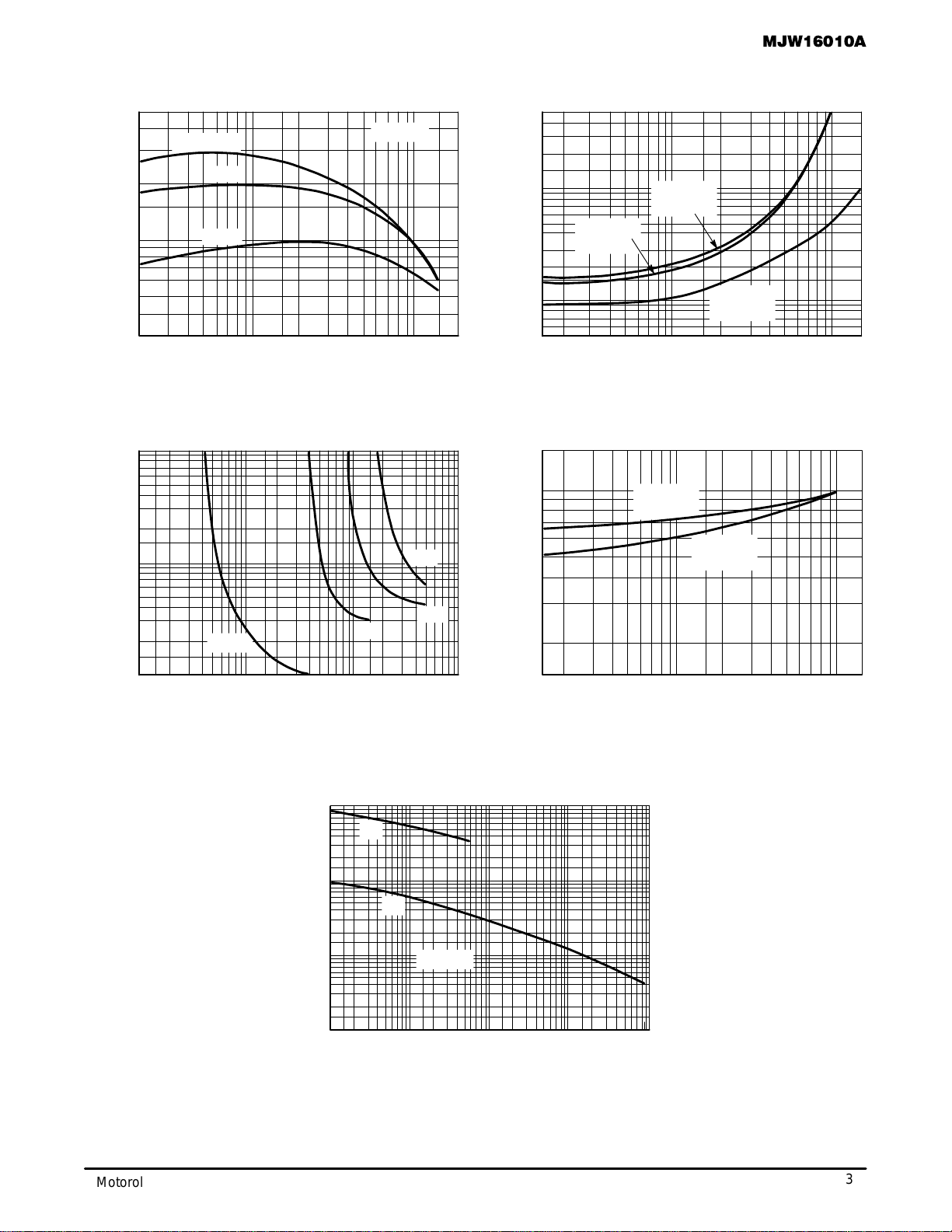
0.15
IC, COLLECTOR CURRENT (AMPS)
0.2 1
1.5
0.5
10
IB, BASE CURRENT (AMPS)
5
2
1
0.5
0.2
0.1 0.15
IC/IB = 10
TJ = 25
°
C
0.2
Figure 1. DC Current Gain
IC, COLLECTOR CURRENT (AMPS)
3
0.2 0.3 0.5 1 2 5 10 20
30
10
7
Figure 2. Collector–Emitter Saturation Region
0.15
IC, COLLECTOR CURRENT (AMPS)
0.05
0.3 1
2
0.5
0.3
50
h
FE
, DC CURRENT GAIN
5
VCE = 5 V
3 5 10 15
Figure 3. Collector–Emitter Saturation Region
50.50.01 0.02 0.05 0.2 0.5 102 50.1
Figure 4. Base–Emitter Saturation Region
Figure 5. Capacitance
5
3
1
10 k
1
VR, REVERSE VOLTAGE (VOLTS)
10
10
2 k
100 850
20
15 A
IC = 1 A
TC = 25°C
C
ib
5 A
TJ = 100°C
–55°C
25°C
20
23
1
2 15
0.1
0.2
0.1
IC/IB = 5
TJ = 25
°
C
IC/IB = 10
TJ = 100
°
C
0.5
1
0.3
0.2
IC/IB = 10
TJ = 25
°
C
IC/IB = 10
TJ = 100
°
C
5 k
1 k
3 k
50
100
200
300
500
0.3 0.5 2 5 2030 50 500300
0.3 3 10
10 A
C
ob
TYPICAL STATIC CHARACTERISTICS
, COLLECTOR–EMITTER VOLTAGE (VOLTS)
CE
V
, COLLECTOR–EMITTER VOLTAGE (VOLTS)
CE
V
, BASE–EMITTER VOLTAGE (VOLTS)
BE
V
C, CAPACITANCE (pF)
 Loading...