

MOTOROLA MJE371 Datasheet
1
Motorola Bipolar Power Transistor Device Data
. . . designed for use in general–purpose amplifier and switching circuits. Recommended for use in 5 to 20 Watt audio amplifiers utilizing complementary symmetry
circuitry.
• DC Current Gain — hFE = 40 (Min) @ IC = 1.0 Adc
• MJE371 is Complementary to NPN MJE521
MAXIMUM RATINGS
Rating
Symbol
Value
Unit
Collector–Emitter Voltage
V
CEO
40
Vdc
Collector–Base Voltage
V
CB
40
Vdc
Emitter–Base Voltage
V
EB
4.0
Vdc
Collector Current — Continuous
— Peak
I
C
4.0
8.0
Adc
Base Current — Continuous
I
B
2.0
Adc
Total Power Dissipation @ TC = 25_C
Derate above 25_C
P
D
40
320
Watts
mW/_C
Operating and Storage Junction Temperature Range
TJ, T
stg
–65 to +150
_
C
THERMAL CHARACTERISTICS
Characteristic
Symbol
Max
Unit
Thermal Resistance, Junction to Case
θ
JC
3.12
_
C/W
ELECTRICAL CHARACTERISTICS (T
C
= 25°C unless otherwise noted)
Characteristic
Symbol
Min
Max
Unit
OFF CHARACTERISTICS
Collector–Emitter Sustaining Voltage (1)
(IC = 100 mAdc, IB = 0)
V
CEO(sus)
40
—
Vdc
Collector–Base Cutoff Current
(VCB = 40 Vdc, IE = 0)
I
CBO
—
100
µAdc
Emitter–Base Cutoff Current
(VEB = 4.0 Vdc, IC = 0)
I
EBO
—
100
µAdc
ON CHARACTERISTICS
DC Current Gain (1)
(IC = 1.0 Adc, VCE = 1.0 Vdc)
h
FE
40
—
—
(1) Pulse Test: Pulse Width v 300 µs, Duty Cycle v 2.0%.
SEMICONDUCTOR TECHNICAL DATA
Order this document
by MJE371/D
Motorola, Inc. 1995
4 AMPERE
POWER TRANSISTOR
PNP SILICON
40 VOLTS
40 WATTS
CASE 77–08
TO–225AA TYPE
REV 2
MJE371
2
Motorola Bipolar Power Transistor Device Data
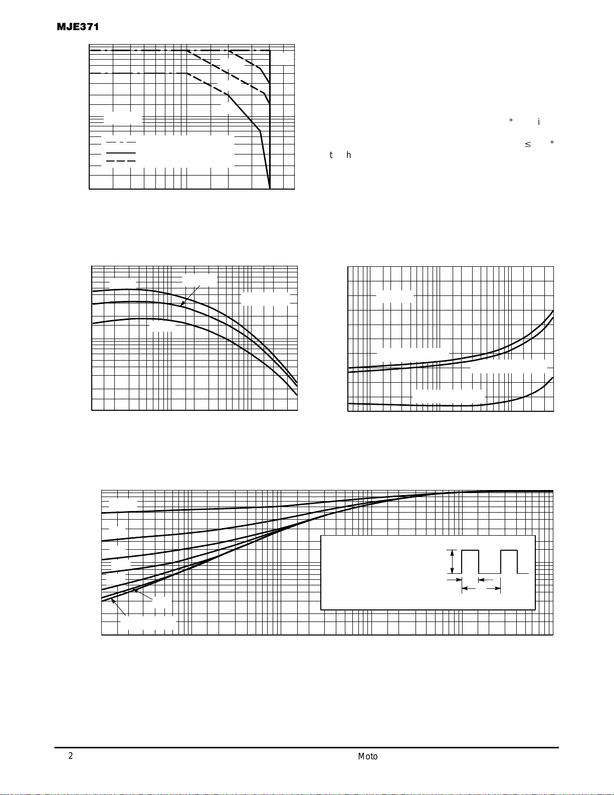
10
VCE, COLLECTOR–EMITTER VOLTAGE (VOLTS)
0.5
40
0.1
0.3
BONDING WIRE LIMIT
SECOND BREAKDOWN LIMIT
THERMAL LIMIT @ TC = 25°C
Figure 1. Active–Region Safe Operating Area
5.0
20106.02.0
TJ = 150°C
I
C
, COLLECTOR CURRENT (AMP)
1.0
2.0
3.0
0.2
604.0 8.0
1.0 ms
dc
100µs
5.0 ms
There are two limitations on the power handling ability of a
transistor: average junction temperature and second breakdown. Safe operating area curves indicate IC – VCE limits of
the transistor that must be observed for reliable operation;
i.e., the transistor must not be subjected to greater dissipation than the curves indicate.
The data of Figure 1 is based on T
J(pk)
= 150_C; TC is variable depending on conditions. Second breakdown pulse limits are valid for duty cycles to 10% provided T
J(pk)
v 150_C.
At high case temperatures, thermal limitations will reduce the
power that can be handled to values less then the limitations
imposed by second breakdown.
IC, COLLECTOR CURRENT (AMP)
h
FE
, DC CURRENT GAIN, NORMALIZED
7.0
10
0.02 0.03 0.1 4.00.01
1.0
0.7
0.5
0.1
0.05 0.3 0.50.2
150°C
TJ = 25°C
–55°C
Figure 2. DC Current Gain Figure 3. “On” Voltage
2.0
IC, COLLECTOR CURRENT (AMP)
1.6
0.4
0
TJ = 25°C
VOLTAGE (VOLTS)
V
BE(sat)
@ IC/IB = 10
V
BE(on)
@ VCE = 1.0 V
5.0
0.3
0.2
1.2
0.8
t, TIME OR PULSE WIDTH (ms)
0.01
0.01 0.03 1.0 2.0 5.0 10 20 50 100 2000.1 0.50.2
1.0
0.2
0.1
0.05
r(t), EFFECTIVE TRANSIENT
θ
JC
(t) = r(t)
θ
JC
θ
JC
= 3.12
°
C/W MAX
D CURVES APPLY FOR POWER
PULSE TRAIN SHOWN
READ TIME AT t
1
T
J(pk)
– TC = P
(pk)
θ
JC
(t)
P
(pk)
t
1
t
2
DUTY CYCLE, D = t1/t
2
SINGLE PULSE
THERMAL RESISTANCE (NORMALIZED)
Figure 4. Thermal Response
0.5
D = 0.5
0.1
0.01
0.3
0.7
0.07
0.03
0.02
3.0
2.0
1.0 3.02.0
VCE = 1.0 Vdc
V
CE(sat)
@ IC/IB = 10
0.01 0.02 0.05 4.00.005 0.03 0.2 0.30.1 0.5 2.0 3.01.0
0.02 0.05 0.3 3.0 500 1000
0.02
0.05
0.2
 Loading...