

Motorola MJ10000 Datasheet
1
Motorola Bipolar Power Transistor Device Data
The MJ10000 Darlington transistor is designed for high–voltage, high–speed,
power switching in inductive circuits where fall time is critical. It is particularly suited
for line operated switchmode applications such as:
• Switching Regulators
• Inverters
• Solenoid and Relay Drivers
• Motor Controls
• Deflection Circuits
100_C Performance Specified for:
Reversed Biased SOA with Inductive Loads
Switching Times With Inductive Loads —
210 ns Inductive Fall Time (Typ)
Saturation Voltages
Leakage Currents
MAXIMUM RATINGS
Rating
Symbol
Value
Unit
Collector–Emitter Voltage
V
CEO
350
Vdc
Collector–Emitter Voltage
V
CEX
400
Vdc
Collector–Emitter Voltage
V
CEV
450
Vdc
Emitter Base Voltage
V
EB
8
Vdc
Collector Current — Continuous
— Peak (1)
I
C
I
CM
20
30
Adc
Base Current — Continuous
— Peak (1)
I
B
I
BM
2.5
5
Adc
Total Power Dissipation @ TC = 25_C
@ TC =100_C
Derate above 25_C
P
D
175
100
1
Watts
W/_C
Operating and Storage Junction Temperature Range
TJ, T
stg
–65 to +200
_
C
THERMAL CHARACTERISTICS
Characteristic
Symbol
Max
Unit
Thermal Resistance, Junction to Case
R
θJC
1
_
C/W
Maximum Lead Temperature for Soldering
Purposes: 1/8″ from Case for 5 Seconds
T
L
275
_
C
(1) Pulse Test: Pulse Width = 5 ms, Duty Cycle v 10%.
Designer’s Data for “Worst Case” Conditions — The Designer’s Data Sheet permits the design of most circuits entirely from the information presented. SOA Limit
curves — representing boundaries on device characteristics — are given to facilitate “worst case” design.
SEMICONDUCTOR TECHNICAL DATA
Order this document
by MJ10000/D
Motorola, Inc. 1995
20 AMPERE
NPN SILICON
POWER DARLINGTON
TRANSISTORS
350 VOLTS
175 WATTS
CASE 1–07
TO–204AA
(TO–3)
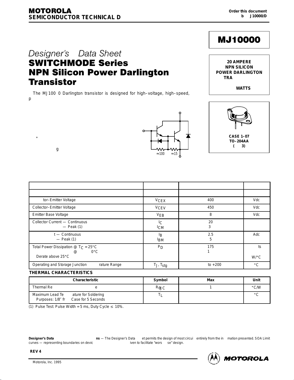
≈
100≈ 15
REV 4
MJ10000
2
Motorola Bipolar Power Transistor Device Data
ELECTRICAL CHARACTERISTICS (T
C
= 25_C unless otherwise noted)
Characteristic
Symbol
Min
Typ
Max
ÎÎÎ
ÎÎÎ
ÎÎÎ
Unit
OFF CHARACTERISTICS (2)
Collector–Emitter Sustaining Voltage (Table 1)
(IC = 250 mA, IB = 0, V
clamp
= Rated V
CEO
) MJ10000
V
CEO(sus)
350
—
—
ÎÎÎ
ÎÎÎ
ÎÎÎ
ÎÎÎ
Vdc
Collector–Emitter Sustaining Voltage (Table 1, Figure 12)
IC = 2 A, V
clamp
= Rated V
CEX
, TC = 100_C MJ10000
IC = 10 A, V
clamp
= Rated V
CEX
, TC = 100_C MJ10000
V
CEX(sus)
400
275
—
—
—
—
ÎÎÎ
ÎÎÎ
ÎÎÎ
ÎÎÎ
ÎÎÎ
Vdc
Collector Cutoff Current
(V
CEV
= Rated Value, V
BE(off)
= 1.5 Vdc)
(V
CEV
= Rated Value, V
BE(off)
= 1.5 Vdc, TC = 150_C)
I
CEV
—
—
—
—
0.25
5
ÎÎÎ
ÎÎÎ
ÎÎÎ
ÎÎÎ
mAdc
Collector Cutoff Current
(VCE = Rated V
CEV
, RBE = 50 Ω, TC = 100_C)
I
CER
—
—
5
ÎÎÎ
ÎÎÎ
ÎÎÎ
ÎÎÎ
mAdc
Emitter Cutoff Current
(VEB = 8 Vdc, IC = 0)
I
EBO
—
—
150
ÎÎÎ
ÎÎÎ
ÎÎÎ
ÎÎÎ
mAdc
SECOND BREAKDOWN
Second Breakdown Collector Current with base forward biased
I
S/b
See Figure 11
ÎÎÎ
ÎÎÎ
ÎÎÎ
Adc
ON CHARACTERISTICS (2)
DC Current Gain
(IC = 5 Adc, VCE = 5 Vdc)
(IC = 10 Adc, VCE = 5 Vdc)
h
FE
50
40
—
—
600
400
ÎÎÎ
ÎÎÎ
ÎÎÎ
ÎÎÎ
ÎÎÎ
—
Collector–Emitter Saturation Voltage
(IC = 10 Adc, IB = 400 mAdc)
(IC = 20 Adc, IB = 1 Adc)
(IC = 10 Adc, IB = 400 mAdc, TC = 100_C)
V
CE(sat)
—
—
—
—
—
—
1.9
3
2
ÎÎÎ
ÎÎÎ
ÎÎÎ
ÎÎÎ
ÎÎÎ
Vdc
Base–Emitter Saturation Voltage
(IC = 10 Adc, IB = 400 mAdc)
(IC = 10 Adc, IB = 400 mAdc, TC = 100_C)
V
BE(sat)
—
—
—
—
2.5
2.5
ÎÎÎ
ÎÎÎ
ÎÎÎ
ÎÎÎ
Vdc
Diode Forward Voltage (1)
(IF = 10 Adc)
V
f
—
3
5
ÎÎÎ
ÎÎÎ
ÎÎÎ
ÎÎÎ
Vdc
DYNAMIC CHARACTERISTICS
Small–Signal Current Gain
(IC = 1.0 Adc, VCE = 10 Vdc, f
test
= 1 MHz)
h
fe
10
—
ÎÎÎ
ÎÎÎ
ÎÎÎ
ÎÎÎ
—
Output Capacitance
(VCB = 10 Vdc, IE = 0, f
test
= 100 kHz)
C
ob
100
325
ÎÎÎ
ÎÎÎ
ÎÎÎ
ÎÎÎ
pF
SWITCHING CHARACTERISTICS
Resistive Load (Table 1)
Delay Time (VCC = 250 Vdc, IC = 10 A,
Rise Time IB1 = 400 mA, V
BE(off)
= 5 Vdc, tp = 50 µs,
Storage Time Duty Cycle v 2%)
Fall Time
t
d
t
r
t
s
t
f
—
—
—
—
0.12
0.20
1.5
1.1
0.2
0.6
3.5
2.4
ÎÎÎ
ÎÎÎ
ÎÎÎ
ÎÎÎ
ÎÎÎ
µs
µs
µs
µs
Inductive Load, Clamped (Table 1)
Storage Time (IC = 10 A(pk), V
clamp
= Rated V
CEX
, IB1 = 400 mA,
Crossover Time V
BE(off)
= 5 Vdc, TC = 100_C)
t
sv
t
c
—
—
3.5
1.5
5.5
3.7
ÎÎÎ
ÎÎÎ
ÎÎÎ
ÎÎÎ
µs
µs
Storage Time (IC = 10 A(pk), V
clamp
= Rated V
CEX
, IB1 = 400 mA,
Crossover Time V
BE(off)
= 5 Vdc, TC = 25_C)
t
sv
t
c
—
—
1.0
0.7
—
—
ÎÎÎ
ÎÎÎ
ÎÎÎ
µs
µs
(1) The internal Collector–to–Emitter diode can eliminate the need for an external diode to clamp inductive loads.
(1) Tests have shown that the Forward Recovery Voltage (Vf) of this diode Is comparable to that of typical fast recovery rectifiers.
(2) Pulse Test: Pulse Width = 300 µs, Duty Cycle v 2%.
MJ10000
3
Motorola Bipolar Power Transistor Device Data
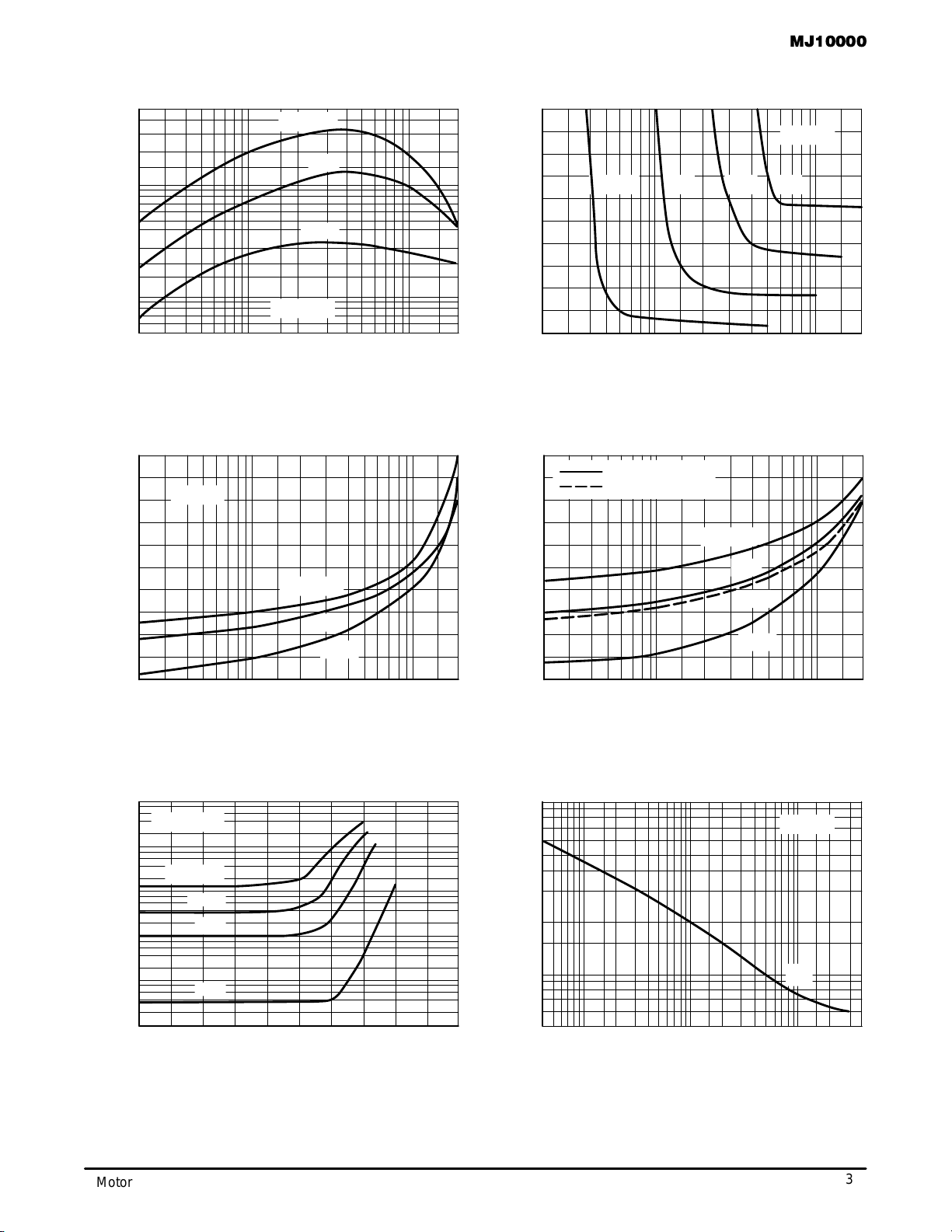
Figure 1. DC Current Gain
IC, COLLECTOR CURRENT (AMP)
5
0.2 0.3 1 2 3
100
50
Figure 2. Collector Saturation Region
V, VOLTAGE (VOLTS)
3
IB, BASE CURRENT (ANP)
1
0.02 0.03 0.1 0.2 0.5 1 2
2.6
2.2
1.8
1.4
IC = 5 A
TJ = 25°C
10 A
VBE, BASE-EMITTER VOLTAGE (VOLTS)
10
4
10
3
10
2
10
1
500
70
h
FE
, DC CURRENT GAIN
TJ = 150°C
VCE = 5 V
, COLLECTOR CURRENT ( A)I
C
10
0
0 +0.2–0.2
VCE = 250 V
TJ = 125°C
100°C
25°C
30
20
10
7
0.5 0.7 5 7 20
Figure 3. Collector Emitter Saturation Voltages
2.4
0.2
IC, COLLECTOR CURRENT (AMPS)
0.4
0.3 0.5 0.7 1 2 5 20
2
1.6
1.2
0.8
IC/IB = 25
TJ = – 55°C
73
Figure 4. Base-Emitter Voltage
2.8
IC, COLLECTOR CURRENT (AMP)
0.8
0.2 0.3 0.5 0.7
2.4
2
1.6
1.2
Figure 5. Collector Cutoff Region
0.4
Figure 6. Output Capacitance
VR, REVERSE VOLTAGE (VOLTS)
50
1 2 20 60100.6
200
70
TJ = 25°C
C
ob
1000
500
100
100 200 400
25°C
–55°C
200
300
10
15 A 20 A
0.05 0.70.30.07
V, VOLTAGE (VOLTS)
10
25°C
150°C
2 5 2073 101
25°C
150°C
25°C
TJ = 55°C
V
BE(sat)
@ IC/IB = 25
V
BE(on)
@ VCE = 3 V
75°C
µ
10
–1
+0.4 +0.8+0.6
4 6 40
700
300
C
ob
, OUTPUT CAPACITANCE (pF)
DC CHARACTERISTICS
, COLLECTOR–EMITTER VOLTAGE (VOLTS)
CE
V
 Loading...