

Motorola MHW5382A Datasheet
1
MHW5382AMOTOROLA RF DEVICE DATA
The RF Line
. . . designed specifically for 450 MHz CATV applications. Features ion–implanted arsenic emitter transistors with 7.0 GHz fT and an all gold metallization
system.
• Specified for 53– and 60–Channel Performance
• Broadband Power Gain @ f = 40–450 MHz
Gp= 38 dB (Typ)
• Broadband Noise Figure
NF = 4.0 dB (Typ)
• Superior Gain, Return Loss and DC Current Stability with Temperature
• All Gold Metallization
• 7.0 GHz Ion–Implanted Transistors
ABSOLUTE MAXIMUM RATINGS
Rating Symbol Value Unit
RF Voltage Input (Single Tone) V
in
+55 dBmV
DC Supply Voltage V
CC
+28 Vdc
Operating Case Temperature Range T
C
–20 to +100 °C
Storage Temperature Range T
stg
–40 to +100 °C
ELECTRICAL CHARACTERISTICS (V
CC
= 24 Vdc, TC = +30°C, 75 Ω system unless otherwise noted)
Characteristic
Symbol Min Typ Max Unit
Frequency Range BW 40 — 450 MHz
Power Gain — 50 MHz G
p
37 38 39.5 dB
Power Gain — 450 MHz G
p
38 39 40 dB
Slope S 0 +1.0 +2.5 dB
Gain Flatness (Peak To Valley) — — 0.3 0.6 dB
Return Loss — Input/Output 40–450 MHz
(Zo = 75 Ohms)
IRL/ORL 18 — — dB
Second Order Intermodulation Distortion
(V
out
= +46 dBmV per ch., Ch 2, M6, M15)
(V
out
= +46 dBmV per ch., Ch 2, M13, M22)
IMD
—
—
–78
–72
—
–64
dB
Cross Modulation Distortion 53–Channel FLAT
(V
out
= +46 dBmV) 60–Channel FLAT
XMD
53
XMD
60
— –63
–61
—
–59
dB
Composite Triple Beat 53–Channel FLAT
(V
out
= +46 dBmV) 60–Channel FLAT
CTB
53
CTB
60
—
—
–63
–60
—
–59
dB
DIN (European Applications Only)
300 MHz — (CH V + Q – P @ W)
400 MHz— (CH M8 + M15 – M9 @ M14)
450 MHz — (CH M20 + M23 – M22 @ M21)
DIN1
DIN2
DIN3
—
—
—
125
124
123
—
—
—
dBµV
Noise Figure
(f = 450 MHz)
NF — 4.0 5.0 dB
DC Current I
DC
— 310 340 mA
Order this document
by MHW5382A/D
SEMICONDUCTOR TECHNICAL DATA
Motorola, Inc. 1994
38 dB GAIN
450 MHz
60–CHANNEL
CATV LINE EXTENDER
AMPLIFIER
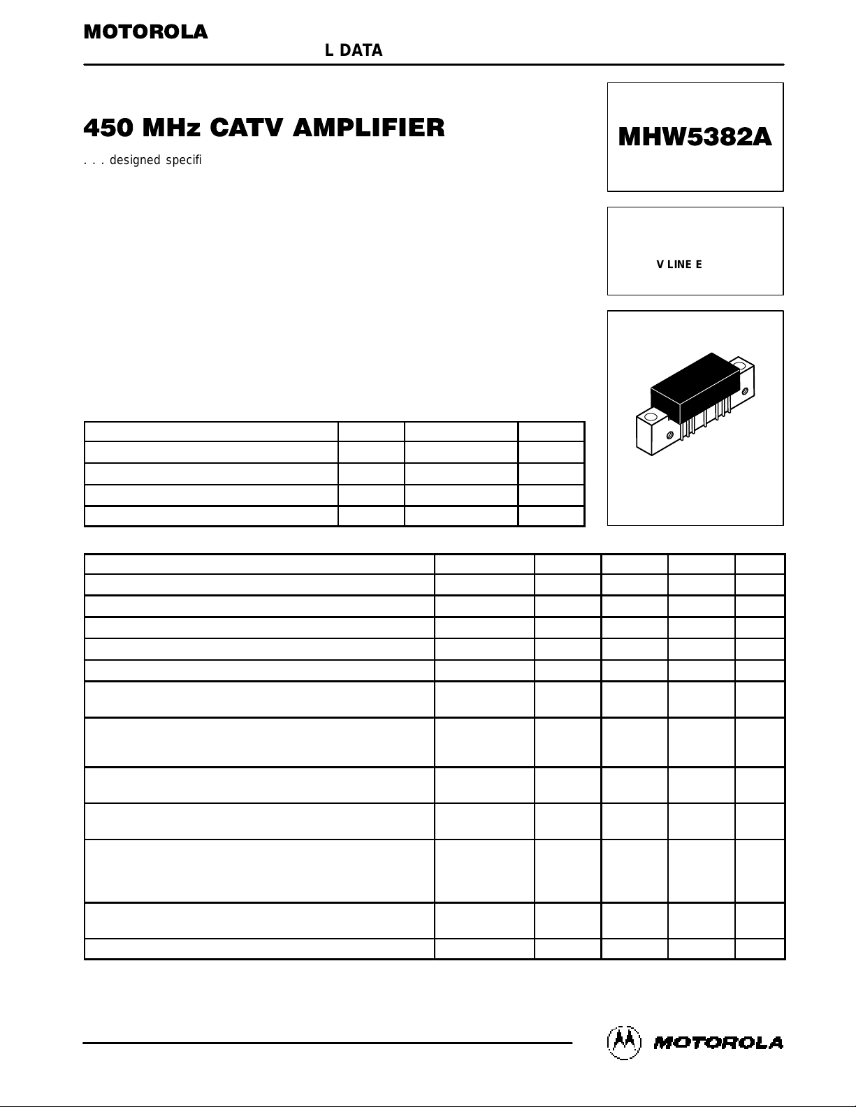
CASE 714–06, STYLE 1
MHW5382A
2
MOTOROLA RF DEVICE DATA
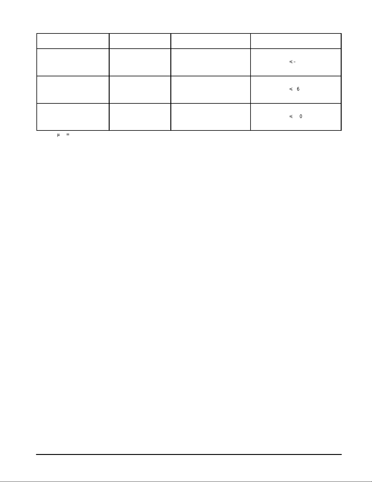
*DIN (European Applications Only)
NCTA Channel
Designation
Frequency
(MHz)
DIN Output Level
(dBmV)**(Typ)
DIN Beat Level
dB Relative to Ref. Ch.
P
Q
V
W (Ref.)
253.25
259.25
289.25
295.25
+59
+59
+65
+65
¬
–60
M8
M9
M14 (Ref.)
M15
361.25
367.25
397.25
403.25
+58
+58
+64
+64
¬
–60
M20
M21 (Ref.)
M22
M23
433.25
439.25
445.25
451.25
+57
+57
+63
+63
¬
–60
**DIN (dBmV) = Reference Channel Level (dBmV) +60 dB
 Loading...