

Motorola MHW2707-1 Datasheet
SEMICONDUCTOR TECHNICAL DATA
The RF Line
Designed for 7.5 volt UHF power amplifier applications in industrial and
commercial equipment primarily for hand portable radios.
• Specified 7.5 Volt Characteristics:
RF Input Power: 1 mW (0 dBm)
RF Output Power: 7 W
Minimum Gain (V
Harmonics: –40 dBc Max @ 2 f
• Meets European Transient Specification (ETS 300 113)
• Epoxy Glass PCB Construction Gives Consistent Performance
and Reliability
• 50 Ω Input/Output Impedances
• Guaranteed Stability and Ruggedness
= 7 V): 38.5 dB
cont
o
Order this document
by MHW2707/D
7 W
403–440 MHz
UHF POWER AMPLIFIER
MAXIMUM RATINGS
DC Supply Voltage (Pins 2, 4, 5) V
DC Control Voltage (Pin 3) V
RF Input Power P
RF Output Power (V
Operating Case Temperature Range T
Storage Temperature Range T
(Flange Temperature = 25°C)
Rating
DD1, 2, 3
= 9 V) P
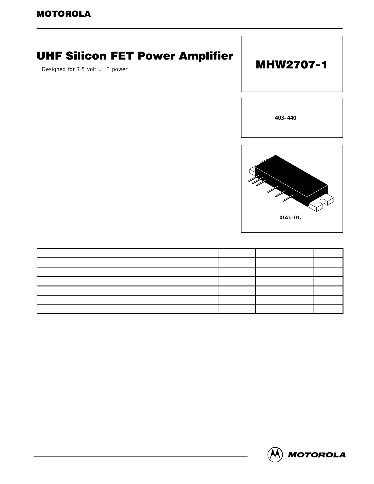
CASE 301AL–01, STYLE 1
Symbol Value Unit
DD1, 2, 3
cont
in
out
C
stg
9 Vdc
7 Vdc
2 mW
9 W
–30 to +80 °C
–30 to +80 °C
REV 1
Motorola, Inc. 1997
MHW2707–1MOTOROLA RF DEVICE DATA
1

ELECTRICAL CHARACTERISTICS (V
noted)
Characteristic
Frequency Range BW 403 440 MHz
Control Voltage
(P
= 7 W; Pin = 1 mW) (1)
out
Quiescent Current
(V
= V
DD1
Power Gain
(P
= 7 W, V
out
Efficiency
(P
= 7 W; Pin = 1 mW) (1)
out
Harmonics (P
Input VSWR
(P
= 7 W; Pin = 1 mW, 50 Ω Ref.) (1)
out
Control Current
(V
= V
DD1
Load Mismatch Stress (V
P
= 9 W; Load VSWR = 10:1, All Phase Angles at Frequency of Test) (1)
out
Stability (Pin = 1–2 mW; V
P
= between 0.1 mW and 9 W; Load VSWR = 8:1,
out
All Phase Angles at Frequency of Test) (1)
(1) Adjust V
= V
DD2
cont
= 7 W; Pin = 1 mW) (1) 2 f
out
= V
DD2
for Specified P
cont
= 7.5 Vdc; Pin = 0 mW, V
DD3
= 7 Vdc)
= 7.5 Vdc; Pin = 1 mW) (1)
DD3
= V
DD1
DD1
out
= V
.
DD2
DD2
= V
DD1
= V
= 9 Vdc; Pin = 2 mW;
DD3
= V
= 6–9 Vdc;
DD3
DD2
cont
= V
DD3
= 0 Vdc)
o
= 7.5 Vdc (Pins 2, 4, 5); TC = +25°C, 50 ohm system unless otherwise
Symbol Min Max Unit
V
cont
— — 1 mA
G
p
η 40 — %
— — –40 dBc
VSWR
in
I
cont
ψ No Degradation in Output
— All Spurious Outputs
0 7 Vdc
38.5 — dB
— 2:1 —
— 2 mA
Power Before & After Test
More Than 60 dB
Below Desired Signal
1
C1
Z1
RF INPUT V
2
C2
L1
C1
DD1
Pin Designations:
Pin 1 — RF Input Power (0 dBm)
Pin 2 — V
Pin 3 — V
Pin 4 — V
Pin 5 — V
Pin 6 — RF OUT (7 Watts nom.)
(7.5 Vdc)
DD1
(0 – 7 Vdc)
cont
(7.5 Vdc)
DD2
(7.5 Vdc)
DD3
MHW2707–1 CIRCUIT BLOCK DIAGRAM
C2
3
L1 L1 L1
C1
V
cont
C2
4
V
DD2
5
V
C3
C1
DD3
C2
C1
Element Values:
C1 = 0.018 µF
C2 = 0.1 µF
C3 = 3.3 µF
L1 = 0.22 µH CHOKE
Z1 = Z2 = 50 Ω Microstrip Line
6
Z2
RF OUTPUT
MHW2707–1
2
Figure 1. UHF Power Module T est Circuit Schematic and Device Block Diagram
MOTOROLA RF DEVICE DATA
 Loading...