

Motorola MHPM7B8A120A Datasheet
SEMICONDUCTOR TECHNICAL DATA
Order this document
by MHPM7B8A120A/D
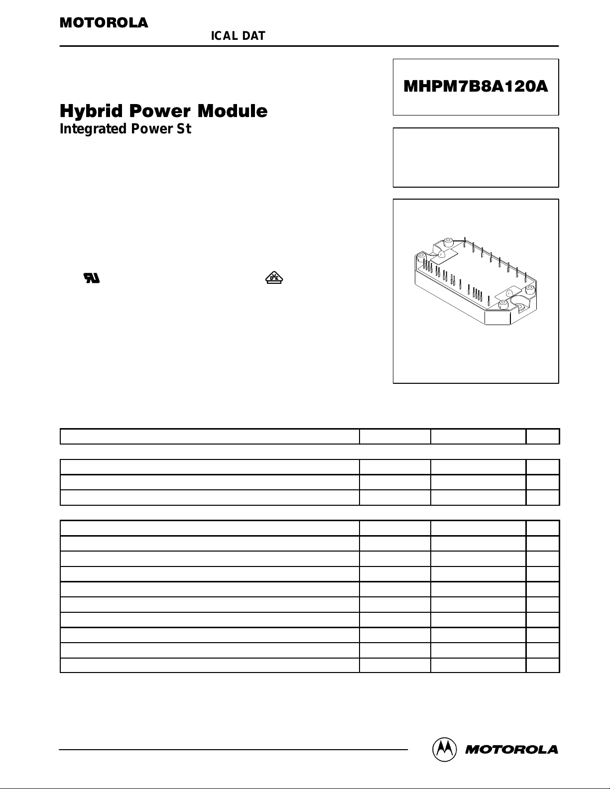
Integrated Power Stage for 1.0 hp Motor Drives
This module integrates a 3–phase input rectifier bridge, 3–phase output
inverter and brake transistor/diode in a single convenient package. The output
inverter utilizes advanced insulated gate bipolar transistors (IGBT) matched
with free–wheeling diodes to give optimal dynamic performance. It has been
configured for use as a three–phase motor drive module or for many other
power switching applications. The top connector pins have been designed for
easy interfacing to the user’s control board.
• Short Circuit Rated 10 µs @ 25°C
• Pin-to-Baseplate Isolation Exceeds 2500 V ac (rms)
• Convenient Package Outline
• UL
• Access to Positive and Negative DC Bus
Recognized and Designed to Meet VDE
Motorola Preferred Device
8.0 AMP, 1200 VOLT
HYBRID POWER MODULE
PLASTIC PACKAGE
CASE 440-01, Style 1
MAXIMUM DEVICE RATINGS (TJ = 25°C unless otherwise noted)
Rating Symbol Value Unit
INPUT RECTIFIER BRIDGE
Repetitive Peak Reverse Voltage V
Average Output Rectified Current (1) I
Peak Non-repetitive Surge Current I
OUTPUT INVERTER
IGBT Reverse Voltage V
Gate-Emitter Voltage V
Continuous IGBT Collector Current I
Peak IGBT Collector Current – (PW = 1.0 ms) (2) I
Continuous Free-Wheeling Diode Current I
Peak Free-Wheeling Diode Current – (PW = 1.0 ms) (2) I
IGBT Power Dissipation P
Free-Wheeling Diode Power Dissipation P
IGBT Junction Temperature Range T
Free-Wheeling Diode Junction Temperature Range T
(1) 1 cycle = 50 or 60 Hz
(2) 1 ms = 1.0% duty cycle
Preferred devices are Motorola recommended choices for future use and best overall value.
RRM
O
FSM
CES
GES
C
C(pk)
F
F(pk)
D
D
J
J
1200 V
8.0 A
200 A
1200 V
± 20 V
8.0 A
16 A
8.0 A
16 A
50 W
30 W
– 40 to +125 °C
– 40 to +125 °C
Motorola, Inc. 1995
MOTOROLA
MHPM7B8A120A
1

MAXIMUM DEVICE RATINGS (continued) (TJ = 25°C unless otherwise noted)
Rating Symbol Value Unit
BRAKE CIRCUIT
IGBT Reverse Voltage V
Gate-Emitter Voltage V
Continuous IGBT Collector Current I
Peak IGBT Collector Current (PW = 1.0 ms) (2) I
IGBT Power Dissipation PD 50 W
Diode Reverse Voltage V
Continuous Output Diode Current I
Peak Output Diode Current (PW = 1.0 ms) (2) I
TOTAL MODULE
Isolation Voltage – (47–63 Hz, 1.0 Minute Duration) V
Ambient Operating Temperature Range T
Operating Case Temperature Range T
Storage Temperature Range T
Mounting Torque – 6.0 lb–in
CES
GES
C
C(pk)
RRM
F
F(pk)
ISO
A
C
stg
1200 V
± 20 V
8.0 A
16 A
1200 V
8.0 A
16 A
2500 VAC
– 40 to + 85 °C
– 40 to + 90 °C
– 40 to +150 °C
ELECTRICAL CHARACTERISTICS (TJ = 25°C unless otherwise noted)
Characteristic Symbol Min Typ Max Unit
INPUT RECTIFIER BRIDGE
Reverse Leakage Current (V
Forward Voltage (IF = 8.0 A) V
Thermal Resistance (Each Die) R
OUTPUT INVERTER
Gate-Emitter Leakage Current (VCE = 0 V, VGE = ± 20 V) I
Collector-Emitter Leakage Current (VCE = 1200 V, VGE = 0 V)
Gate-Emitter Threshold Voltage (VCE = VGE, IC = 1.0 mA) V
Collector-Emitter Breakdown Voltage (IC = 10 mA, VGE = 0) V
Collector-Emitter Saturation Voltage (VGE = 15 V, IC = 8.0 A) V
Input Capacitance (VGE = 0 V, VCE = 25 V, f = 1.0 MHz) Cies – 1000 – pF
Input Gate Charge (VCE = 600 V, IC = 8.0 A, VGE = 15 V) Q
Fall Time – Inductive Load
(VCE = 600 V, IC = 8.0 A, VGE = 15 V, RG = 150 Ω)
Turn-On Energy
(VCE = 600 V, IC = 8.0 A, VGE = 15 V, RG = 150 Ω)
Turn-Off Energy
(VCE = 600 V, IC = 8.0 A, VGE = 15 V, RG = 150 Ω)
Diode Forward Voltage (IF = 8.0 A, VGE = 0 V) V
Diode Reverse Recovery Time
(IF = 8.0 A, V = 600 V, dI/dt = 50 A/µs)
Diode Stored Charge (IF = 8.0 A, V = 600 V, di/dt = 50 A/µs) Q
Thermal Resistance – IGBT (Each Die) R
Thermal Resistance – Free-Wheeling Diode (Each Die) R
(2) 1.0 ms = 1.0% duty cycle
= 1200 V) I
RRM
TJ = 25°C
TJ = 125°C
R
F
θJC
GES
I
CES
GE(th)
(BR)CES
CE(SAT)
T
t
fi
E
(on)
E
(off)
F
t
rr
rr
θJC
θJC
– 10 50 µA
– 1.05 1.5 V
– – 2.9 °C/W
– – ± 20 µA
–
–
4.0 6.0 8.0 V
1200 1300 – V
– 2.5 3.5 V
– 75 – nC
– 350 500 ns
– – 1.0 mJ
– – 1.0 mJ
– 1.6 2.2 V
– 140 200 ns
– – 900 nC
– – 2.2 °C/W
– – 3.7 °C/W
–
–
100
500
µA
µA
MHPM7B8A120A
2
MOTOROLA

ELECTRICAL CHARACTERISTICS
Characteristic Symbol Min Typ Max Unit
BRAKE CIRCUIT
Gate-Emitter Leakage Current (VCE = 0 V, VGE = ± 20 V) I
Collector-Emitter Leakage Current (VCE = 1200 V, VGE = 0 V)
Gate-Emitter Threshold Voltage (VCE = VGE, IC = 1.0 mA) V
Collector-Emitter Breakdown Voltage (IC = 10 mA, VGE = 0) V
Collector-Emitter Saturation Voltage (VGE = 15 V, IC = 8.0 A) V
Input Capacitance (VGE = 0 V, VCE = 10 V, f = 1.0 MHz) Cies – 1000 – pF
Input Gate Charge (VCE = 600 V, IC = 8.0 A, VGE = 15 V) Q
Fall Time – Inductive Load
(VCE = 600 V, IC = 8.0 A, VGE = 15 V, RG = 150 Ω)
Turn-On Energy
(VCE = 600 V, IC = 8.0 A, VGE = 15 V, RG = 150 Ω)
Turn-Off Energy
(VCE = 600 V, IC = 8.0 A, VGE = 15 V, RG = 150 Ω)
Diode Forward Voltage (IF = 8.0 A) V
Diode Reverse Leakage Current I
Thermal Resistance – IGBT R
Thermal Resistance – Diode R
(continued) (T
TJ = 25°C
TJ = 125°C
= 25°C unless otherwise noted)
J
GES
I
CES
GE(th)
(BR)CES
CE(SAT)
T
t
fi
E
(on)
E
(off)
F
R
θJC
θJC
4.0 6.0 8.0 V
1200 1300 – V
– – ± 20 µA
–
–
– 2.5 3.5 V
– 75 – nC
– 350 500 ns
– – 1.0 mJ
–
– 1.6 2.2 V
– – 50 µA
– – 2.2 °C/W
– – 3.7 °C/W
–
–
–
100
500
1.0 mJ
µA
µA
MOTOROLA
MHPM7B8A120A
3
 Loading...