

MOTOROLA MGY25N120D Datasheet
SEMICONDUCTOR TECHNICAL DATA
Order this document
by MGY25N120D/D
!
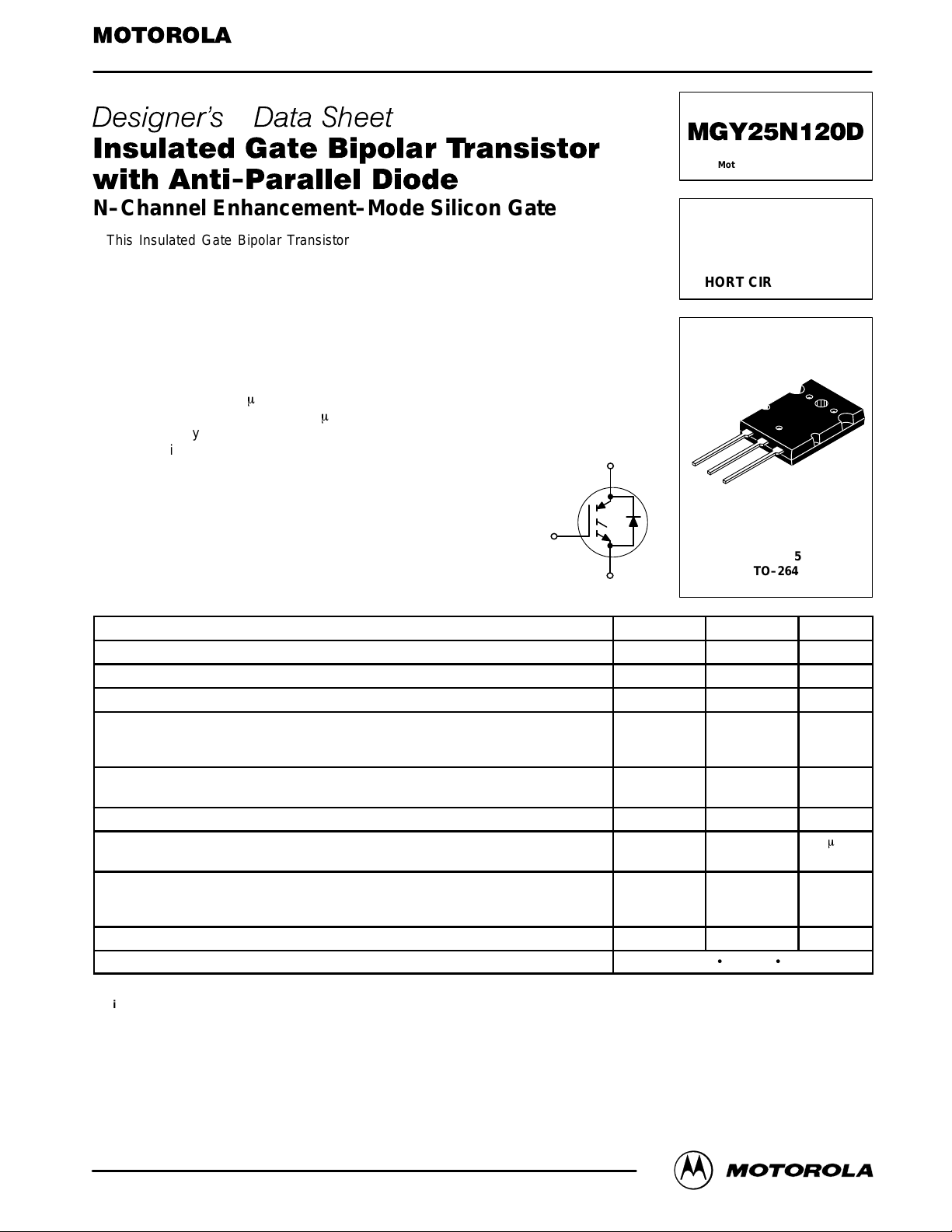
N–Channel Enhancement–Mode Silicon Gate
This Insulated Gate Bipolar Transistor (IGBT) is co–packaged
with a soft recovery ultra–fast rectifier and uses an advanced
termination scheme to provide an enhanced and reliable high
voltage blocking capability . Short circuit rated IGBT’s are specifically suited for applications requiring a guaranteed short circuit
withstand time such as Motor Control Drives. Fast switching
characteristics result in efficient operation at high frequencies.
Co–packaged IGBT’s save space, reduce assembly time and cost.
• Industry Standard High Power TO–264 Package (TO–3PBL)
• High Speed E
• High Short Circuit Capability – 10 ms minimum
• Soft Recovery Free Wheeling Diode is included in the package
• Robust High Voltage Termination
• Robust RBSOA
: 216 mJ/A typical at 125°C
off
G
Motorola Preferred Device
IGBT & DIODE IN TO–264
25 A @ 90°C
38 A @ 25°C
1200 VOL TS
SHORT CIRCUIT RATED
C
E
G
C
E
CASE 340G–02
STYLE 5
TO–264
MAXIMUM RATINGS
Collector–Emitter Voltage V
Collector–Gate Voltage (RGE = 1.0 MΩ) V
Gate–Emitter Voltage — Continuous V
Collector Current — Continuous @ TC = 25°C
Total Power Dissipation @ TC = 25°C
Derate above 25°C
Operating and Storage Junction Temperature Range TJ, T
Short Circuit Withstand Time
(VCC = 720 Vdc, VGE = 15 Vdc, TJ = 125°C, RG = 20 Ω)
Thermal Resistance — Junction to Case – IGBT
Maximum Lead Temperature for Soldering Purposes, 1/8″ from case for 5 seconds T
Mounting Torque, 6–32 or M3 screw
(1) Pulse width is limited by maximum junction temperature. Repetitive rating.
Designer’s Data for “Worst Case” Conditions — The Designer’s Data Sheet permits the design of most circuits entirely from the information presented. SOA Limit
curves —representing boundaries on device characteristics — are given to facilitate “worst case” design.
Designer’s is a trademark of Motorola, Inc.
(TJ = 25°C unless otherwise noted)
Rating Symbol Value Unit
— Continuous @ TC = 90°C
— Repetitive Pulsed Current (1)
— Junction to Case – Diode
— Junction to Ambient
CES
CGR
GE
I
C25
I
C90
I
CM
P
D
stg
t
sc
R
θJC
R
θJC
R
θJA
L
10 lbfSin (1.13 NSm)
1200 Vdc
1200 Vdc
±20 Vdc
38
25
76
212
1.69
–55 to 150 °C
10
0.6
0.9
35
260 °C
Adc
Apk
Watts
W/°C
m
°C/W
s
Preferred devices are Motorola recommended choices for future use and best overall value.
REV 2
Motorola IGBT Device Data
Motorola, Inc. 1997
1
MGY25N120D
)
f = 1.0 MHz)
)
R
G
Ω)
)
R
G
T
J
125 C)
)
V
GE
Vdc)
ELECTRICAL CHARACTERISTICS
OFF CHARACTERISTICS
Collector–to–Emitter Breakdown Voltage
(VGE = 0 Vdc, IC = 25 µAdc)
T emperature Coef ficient (Positive)
Zero Gate Voltage Collector Current
(VCE = 1200 Vdc, VGE = 0 Vdc)
(VCE = 1200 Vdc, VGE = 0 Vdc, TJ = 125°C)
Gate–Body Leakage Current (VGE = ± 20 Vdc, VCE = 0 Vdc) I
ON CHARACTERISTICS (1)
Collector–to–Emitter On–State Voltage
(VGE = 15 Vdc, IC = 12.5 Adc)
(VGE = 15 Vdc, IC = 12.5 Adc, TJ = 125°C)
(VGE = 15 Vdc, IC = 25 Adc)
Gate Threshold Voltage
(VCE = VGE, IC = 1.0 mAdc)
Threshold Temperature Coefficient (Negative)
Forward Transconductance (VCE = 10 Vdc, IC = 20 Adc) g
DYNAMIC CHARACTERISTICS
Input Capacitance
Output Capacitance
Transfer Capacitance
SWITCHING CHARACTERISTICS (1)
Turn–On Delay Time
Rise Time
Turn–Off Delay Time
Fall Time
Turn–Off Switching Loss
Turn–On Switching Loss E
Total Switching Loss E
Turn–On Delay Time
Rise Time
Turn–Off Delay Time
Fall Time
Turn–Off Switching Loss
Turn–On Switching Loss E
Total Switching Loss E
Gate Charge
DIODE CHARACTERISTICS
Diode Forward Voltage Drop
(IEC = 12.5 Adc)
(IEC = 12.5 Adc, TJ = 125°C)
(IEC = 25 Adc)
(1) Pulse Test: Pulse Width ≤300 µs, Duty Cycle ≤ 2%. (continued)
(T
= 25°C unless otherwise noted)
J
Characteristic
(VCE = 25 Vdc, VGE = 0 Vdc,
(VCC = 720 Vdc, IC = 25 Adc,
VGE = 15 Vdc, L = 300 mH
Energy losses include “tail”
(VCC = 720 Vdc, IC = 25 Adc,
VGE = 15 Vdc, L = 300 mH
Energy losses include “tail”
(VCC = 720 Vdc, IC = 25 Adc,
R
= 20 Ω, T
= 20 Ω,
f = 1.0 MHz
R
= 20 Ω
= 20
V
= 15 Vdc
= 15
= 125°C
=
Symbol Min Typ Max Unit
V
(BR)CES
I
CES
GES
V
CE(on)
V
GE(th)
fe
C
ies
C
oes
C
res
t
d(on)
t
r
t
d(off)
t
f
E
off
on
ts
t
d(on)
t
r
t
d(off)
t
f
E
off
on
ts
Q
T
Q
1
Q
2
V
FEC
1200
—
—
—
— — 250 nAdc
—
—
—
4.0
—
— 12 — Mhos
— 1859 — pF
— 198 —
— 30 —
— 91 — ns
— 124 —
— 196 —
— 310 —
— 2.44 4.69 mJ
— 3.14 5.22
— 5.58 9.91
— 88 — ns
— 126 —
— 236 —
— 640 —
— 5.40 — mJ
— 5.03 —
— 10.43 —
— 62 — nC
— 22 —
— 25 —
—
—
—
—
960
—
—
2.37
2.15
2.98
6.0
10
2.89
1.75
3.65
—
—
100
2500
3.24
—
4.19
8.0
—
3.50
—
4.45
mV/°C
µAdc
mV/°C
Vdc
Vdc
Vdc
Vdc
2
Motorola IGBT Device Data
 Loading...