

Motorola MGW12N120 Datasheet
1
Motorola TMOS Power MOSFET Transistor Device Data
N–Channel Enhancement–Mode Silicon Gate
This Insulated Gate Bipolar Transistor (IGBT) uses an advanced
termination scheme to provide an enhanced and reliable high
voltage–blocking capability. Short circuit rated IGBT’s are specifically suited for applications requiring a guaranteed short circuit
withstand time s uch as M otor C ontrol Drives. Fast switching
characteristics result in efficient operation at high frequencies.
• Industry Standard High Power TO–247 Package with
Isolated Mounting Hole
• High Speed E
off
: 160 mJ/A typical at 125°C
• High Short Circuit Capability – 10 ms minimum
• Robust High Voltage Termination
MAXIMUM RATINGS
(TJ = 25°C unless otherwise noted)
Rating
Symbol Value Unit
Collector–Emitter Voltage V
CES
1200 Vdc
Collector–Gate Voltage (RGE = 1.0 MΩ) V
CGR
1200 Vdc
Gate–Emitter Voltage — Continuous V
GE
±20 Vdc
Collector Current — Continuous @ TC = 25°C
Collector Current — Continuous @ TC = 90°C
Collector Current — Repetitive Pulsed Current (1)
I
C25
I
C90
I
CM
20
12
40
Adc
Apk
Total Power Dissipation @ TC = 25°C
Derate above 25°C
P
D
123
0.98
Watts
W/°C
Operating and Storage Junction Temperature Range TJ, T
stg
–55 to 150 °C
Short Circuit Withstand Time
(VCC = 720 Vdc, VGE = 15 Vdc, TJ = 125°C, RG = 20 Ω)
t
sc
10
m
s
Thermal Resistance — Junction to Case – IGBT
Thermal Resistance — Junction to Ambient
R
θJC
R
θJA
1.0
45
°C/W
Maximum Lead Temperature for Soldering Purposes, 1/8″ from case for 5 seconds T
L
260 °C
Mounting Torque, 6–32 or M3 screw
10 lbfSin (1.13 NSm)
(1) Pulse width is limited by maximum junction temperature. Repetitive rating.
Designer’s Data for “Worst Case” Conditions — The Designer’s Data Sheet permits the design of most circuits entirely from the information presented. SOA Limit
curves — representing boundaries on device characteristics— are given to facilitate “worst case” design.
Preferred devices are Motorola recommended choices for future use and best overall value.
REV 1
Order this document
by MGW12N120/D
SEMICONDUCTOR TECHNICAL DATA
IGBT IN TO–247
12 A @ 90°C
20 A @ 25°C
1200 VOLTS
SHORT CIRCUIT RATED
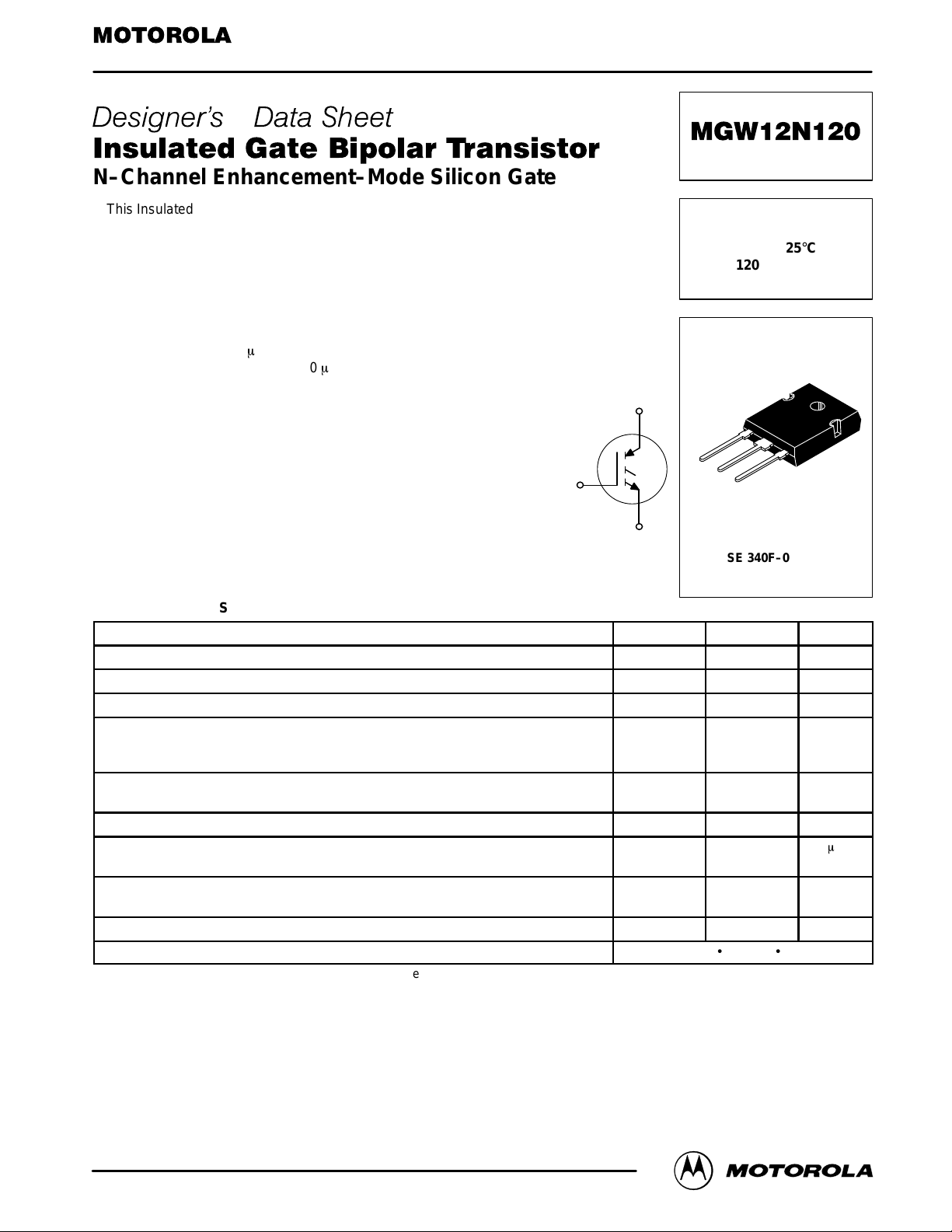
CASE 340F–03, Style 4
TO–247AE
Motorola Preferred Device
G
C
E
C
E
G
Motorola, Inc. 1996
MGW12N120
2
Motorola TMOS Power MOSFET Transistor Device Data
ELECTRICAL CHARACTERISTICS
(T
J
= 25°C unless otherwise noted)
Characteristic
Symbol Min Typ Max Unit
OFF CHARACTERISTICS
Collector–to–Emitter Breakdown Voltage
(VGE = 0 Vdc, IC = 25 µAdc)
Temperature Coefficient (Positive)
BV
CES
1200
—
—
870
—
—
Vdc
mV/°C
Emitter–to–Collector Breakdown Voltage (VGE = 0 Vdc, IEC = 100 mAdc) BV
ECS
25 — — Vdc
Zero Gate Voltage Collector Current
(VCE = 1200 Vdc, VGE = 0 Vdc)
(VCE = 1200 Vdc, VGE = 0 Vdc, TJ = 125°C)
I
CES
—
—
—
—
100
2500
µAdc
Gate–Body Leakage Current (VGE = ± 20 Vdc, VCE = 0 Vdc) I
GES
— — 250 nAdc
ON CHARACTERISTICS (1)
Collector–to–Emitter On–State Voltage
(VGE = 15 Vdc, IC = 5.0 Adc)
(VGE = 15 Vdc, IC = 5.0 Adc, TJ = 125°C)
(VGE = 15 Vdc, IC = 10 Adc)
V
CE(on)
—
—
—
2.51
2.36
3.21
3.37
—
4.42
Vdc
Gate Threshold Voltage
(VCE = VGE, IC = 1.0 mAdc)
Threshold Temperature Coefficient (Negative)
V
GE(th)
4.0
—
6.0
10
8.0
—
Vdc
mV/°C
Forward Transconductance (VCE = 10 Vdc, IC = 10 Adc) g
fe
— 12 — Mhos
DYNAMIC CHARACTERISTICS
Input Capacitance
C
ies
— 930 — pF
Output Capacitance
(VCE = 25 Vdc, VGE = 0 Vdc,
f = 1.0 MHz)
C
oes
— 126 —
Transfer Capacitance
f = 1.0 MHz)
C
res
— 16 —
SWITCHING CHARACTERISTICS (1)
Turn–On Delay Time
t
d(on)
— 74 — ns
Rise Time
t
r
— 83 —
Turn–Off Delay Time
CC
= 720 Vdc, IC = 10 Adc,
VGE = 15 Vdc, L = 300 mH
t
d(off)
— 76 —
Fall Time
m
H
RG = 20 Ω, TJ = 25°C)
Energy losses include “tail”
t
f
— 231 —
Turn–Off Switching Loss
m
H
RG = 20 Ω, TJ = 25°C)
Energy losses include “tail”
E
off
— 0.55 1.33 mJ
Turn–On Delay Time
t
d(on)
— 66 — ns
Rise Time
t
r
— 87 —
Turn–Off Delay Time
CC
= 720 Vdc, IC = 10 Adc,
VGE = 15 Vdc, L = 300 mH
t
d(off)
— 120 —
Fall Time
m
H
RG = 20 Ω, TJ = 125°C)
Energy losses include “tail”
t
f
— 575 —
Turn–Off Switching Loss
m
H
RG = 20 Ω, TJ = 125°C)
Energy losses include “tail”
E
off
— 1.49 — mJ
Q
T
— 31 — nC
(VCC = 720 Vdc, IC = 10 Adc,
V
= 15 Vdc)
Q
1
— 13 —
VGE = 15 Vdc)
Q
2
— 14 —
INTERNAL PACKAGE INDUCTANCE
Internal Emitter Inductance
(Measured from the emitter lead 0.25″ from package to emitter bond pad)
L
E
— 13 —
nH
(1) Pulse Test: Pulse Width ≤ 300 µs, Duty Cycle ≤ 2%.
Gate Charge
(VCC = 720 Vdc, IC = 10 Adc,
(VCC = 720 Vdc, IC = 10 Adc,
 Loading...