

Motorola MGS05N60D Datasheet

SEMICONDUCTOR TECHNICAL DATA
N–Channel Enhancement–Mode Silicon Gate
This IGBT contains a built–in free wheeling diode and a gate
protection zener. Fast switching characteristics result in efficient
operation at higher frequencies.
• Built–In Free Wheeling Diode
• Built–In Gate Protection Zener Diode
• Industry Standard Package (TO92 — 1.0 Watt)
• High Speed E
dV/dt = 1000 V/ms
• Robust High Voltage Termination
• Robust Turn–Off SOA
: Typical 6.5 mJ @ IC = 0.3 A; TC = 125°C and
off
G
Order this document
by MGS05N60D/D
POWERLUX
IGBT
0.5 A @ 25°C
600 V
C
E
C
G
E
MAXIMUM RATINGS
Collector–Emitter Voltage V
Collector–Gate Voltage (RGE = 1.0 MΩ) V
Gate–Emitter Voltage — Continuous V
Collector Current — Continuous @ TC = 25°C
Total Power Dissipation @ TC = 25°C P
Operating and Storage Junction Temperature Range TJ, T
(TC = 25°C unless otherwise noted)
Parameters Symbol Value Unit
— Continuous @ TC = 90°C
— Repetitive Pulsed Current (1)
CES
CGR
GES
I
C25
I
C90
I
CM
D
stg
CASE 029–05
TO–226AE
TO92 (1.0 WATT)
600 Vdc
600 Vdc
±15 Vdc
0.5
0.3
2.0
1.0 Watt
–55 to 150 °C
Adc
THERMAL CHARACTERISTICS
Thermal Resistance — Junction to Case – IGBT
Maximum Lead Temperature for Soldering Purposes, 1/8″ from case for 5 seconds T
UNCLAMPED DRAIN–TO–SOURCE AVALANCHE CHARACTERISTICS (T
Single Pulse Drain–to–Source Avalanche
Energy – Starting @ TC = 25°C
Energy – Starting @ TC = 125°C
VCE = 100 V, VGE = 15 V, Peak IL = 2.0 A, L = 3.0 mH, RG = 25
(1) Pulse width is limited by maximum junction temperature repetitive rating.
Designer’s Data for “Worst Case” Conditions — The Designer’s Data Sheet permits the design of most circuits entirely from the information presented. SOA Limit
curves — representing boundaries on device characteristics — are given to facilitate “worst case” design.
Designer’s is a trademark of Motorola, Inc.
— Junction to Ambient
≤ 150°C)
C
W
R
R
E
θJC
θJA
L
AS
25
125
260 °C
125
40
°C/W
mJ
Motorola Power Products Division Technical Data
Motorola, Inc. 1997
1
MGS05N60D
)
f = 1.0 MHz)
)
T
C
25 C, dV/dt = 1000 V/ms)
)
T
C
125 C, dV/dt = 1000 V/ms)
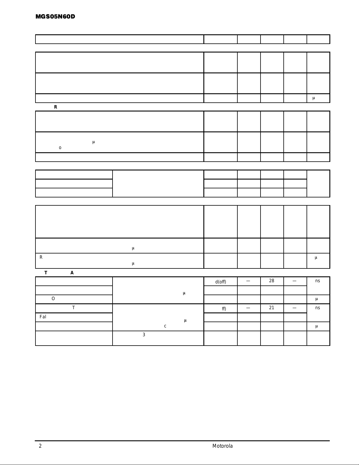
ELECTRICAL CHARACTERISTICS
OFF CHARACTERISTICS
Collector–to–Emitter Breakdown Voltage
(VGE = 0 Vdc, IC = 250 µAdc)
T emperature Coef ficient (Positive)
Zero Gate Voltage Collector Current
(VCE = 600 Vdc, VGE = 0 Vdc, TC = 25°C)
(VCE = 600 Vdc, VGE = 0 Vdc, TC = 125°C)
Gate–Body Leakage Current (VGE = ±15 Vdc, VCE = 0 Vdc) I
ON CHARACTERISTICS
Collector–to–Emitter On–State Voltage
(VGE = 15 Vdc, IC = 0.3 Adc, TC = 25°C)
(VGE = 15 Vdc, IC = 0.3 Adc, TC = 125°C)
Gate Threshold Voltage
(VCE = VGE, IC = 250 mAdc)
Threshold Temperature Coefficient (Negative)
Forward Transconductance (VCE = 10 Vdc, IC = 0.5 Adc) g
DYNAMIC CHARACTERISTICS
Input Capacitance
Output Capacitance
Transfer Capacitance
DIODE CHARACTERISTICS
Diode Forward Voltage Drop
(IEC = 0.3 Adc, TC = 25°C)
(IEC = 0.3 Adc, TC = 125°C)
(IEC = 0.1 Adc, TC = 25°C)
(IEC = 0.1 Adc, TC = 125°C)
Reverse Recovery Time @ TC = 25°C
IF = 0.4 Adc, VR = 300 Vdc, dIF/dt = 10 A/ms
Reverse Recovery Stored Charge
IF = 0.4 Adc, VR = 300 Vdc, dIF/dt = 10 A/ms
SWITCHING CHARACTERISTICS (1)
Turn–Off Delay Time
Fall Time
Turn–Off Switching Loss
Turn–Off Delay Time
Fall Time
Turn–Off Switching Loss
Gate Charge (VCC = 300 Vdc, IC = 0.3 Adc,
(1) Pulse Test: Pulse Width ≤ 300 µs, Duty Cycle ≤ 2%.
(T
= 25°C unless otherwise noted)
C
Characteristic
(VCE = 20 Vdc, VGE = 0 Vdc,
(VCC = 300 Vdc, IC = 0.4 Adc,
VGE = 15 Vdc, L = 3.0 mH, RG = 25 Ω,
T
(VCC = 300 Vdc, IC = 0.4 Adc,
VGE = 15 Vdc, L = 3.0 mH, RG = 25 Ω,
T
f = 1.0 MHz
= 25°C, dV/dt = 1000 V/ms
=
Energy losses include “tail”
= 125°C, dV/dt = 1000 V/ms
=
Energy losses include “tail”
VGE = 15 Vdc)
Symbol Min Typ Max Unit
B
VCES
I
CES
I
CES
GES
V
CE(on)
V
GE(th)
C
C
C
V
FEC
t
Q
t
d(off)
E
t
d(off)
E
Q
fe
ies
oes
res
rr
RR
t
f
off
t
f
off
T
600
—
—
—
— 10 100
—
—
3.5
—
0.3 0.42 — Mhos
— 75 100 pF
— 11 20
— 1.6 5.0
—
—
—
—
— 150 —
— 35 —
— 28 — ns
— 150 —
— 3.25 4.25
— 21 — ns
— 280 —
— 8.0 10
— 6.4 — nC
680
0.7
0.1
5.0
1.6
1.5
—
6.0
5.0
5.2
2.3
2.3
—
—
5.0
50
2.0
—
6.0
—
6.0
—
3.0
—
Vdc
V/°C
µAdc
m
Adc
Vdc
Vdc
mV/°C
Vdc
ns
m
m
m
C
J
J
2
Motorola Power Products Division Technical Data
 Loading...