Motorola MCM72PB8ML3.5, MCM72FB8ML8, MCM72FB8ML8R, MCM72FB8ML7.5R, MCM72PB8ML4R Datasheet
...
MOTOROLA
SEMICONDUCTOR TECHNICAL DATA
Advance Information
256K x 72 Bit BurstRAM
Order this document
by MCM72FB8ML/D
MCM72FB8ML
MCM72PB8ML
Multichip Module
The 256K x 72 multichip module uses four 4M bit synchronous fast static RAMs
designed to provide a burstable, high performance, secondary cache for the
PowerPC and other high performance microprocessors. It is organized as
256K words of 72 bits each. This device integrates input registers, an output register (MCM72PB8ML only), a 2–bit address counter, and high speed SRAM onto
a single monolithic circuit for reduced parts count in cache data RAM applications. Synchronous design allows precise cycle control with the use of an external clock (K). BiCMOS circuitry reduces the overall power consumption of the
integrated functions for greater reliability.
Addresses (SA), data inputs (DQx), and all control signals except output
enable (G
edge–triggered noninverting registers.
addresses can be generated internally (burst sequence operates in linear or
interleaved mode dependent upon the state of LBO
address advance (ADV
clock (K) input. This feature eliminates complex off–chip write pulse generation
and provides increased timing flexibility for incoming signals.
nous write enable (SW
to all bytes. The eight bytes are designated as “a” through “h”. SBa
SBb
are asserted with SW. All bytes are written if either SGW is asserted or if all SBx
and SW are asserted.
For read cycles, pipelined SRAMs output data is temporarily stored by an edge–
triggered output register and then released to the output buffers at the next rising
edge of clock (K). Flow–through SRAMs allow output to simply flow freely from
the memory array.
operate on a separate 2.5 V or 3.3 V power supply. All inputs and outputs are
JEDEC standard JESD8–5 compatible.
• 3.3 V + 10%, – 5% Core Power Supply , 2.5 V or 3.3 V I/O Supply
• ADSP
• Option for Pipeline or Flow–Through (Speeds Guaranteed When Module is
• Selectable Burst Sequencing Order (Linear/Interleaved)
• Single–Cycle Deselect Timing
• Internally Self–Timed Write Cycle
• Byte Write and Global Write Control
• JEDEC BGA Pin Assignment
) and linear burst order (LBO) are clock (K) controlled through positive–
Bursts can be initiated with either ADSP
) input pin.
Write cycles are internally self–timed and are initiated by the rising edge of the
Synchronous byte write (SBx
) are provided to allow writes to either individual bytes or
controls DQb, etc. Individual bytes are written if the selected byte writes SBx
The module can be configured as either a pipelined or flow–through SRAM.
The multichip module operates from a 3.3 V core power supply and all outputs
, ADSC, and ADV Burst Control Pins
Purchased by Appropriate Part Number)
), synchronous global write (SGW), and synchro-
or ADSC input pins. Subsequent burst
) and controlled by the burst
controls DQa,
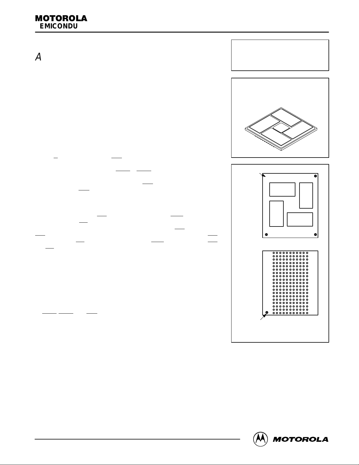
MULTICHIP MODULE
PIN A1
INDICA TION
(corner without
fiducial)
PIN A1
INDICA TION
(corner with
fiducial)
PBGA
CASE 1103B–01
TOP VIEW
BOTTOM VIEW
(Drawings Not to Scale)
The PowerPC name is a trademark of IBM Corp., used under license therefrom.
This document contains information on a new product. Specifications and information herein are subject to change without notice.
REV 1
7/30/97
Motorola, Inc. 1997
MOTOROLA FAST SRAM
MCM72FB8ML MCM72PB8ML
1

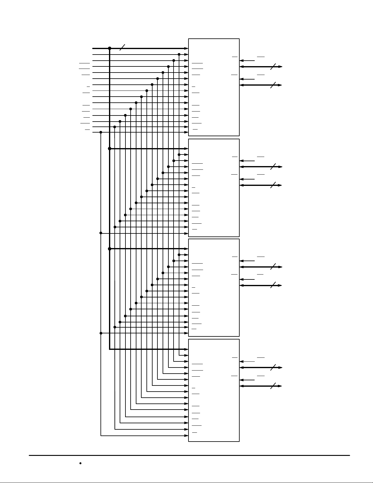
256K X 72 FOUR–CHIP MODULE BLOCK DIAGRAM
SA2 – SA17
SA0
SA1
ADSP
ADSC
ADV
K
G
SE1
SE2
SE3
LBO
SW
SGW
FT
18
MCM69P/F819DC*
SA2 – SA17
SA0
SA1
ADSP
ADSC
ADV
K
G
SE1
SE2
SE3
LBO
SW
SGW
FT
SA2 – SA17
SA0
SA1
ADSP
ADSC
ADV
K
G
SE1
SE2
SE3
LBO
SW
SGW
FT
SA2 – SA17
SA0
SA1
ADSP
ADSC
ADV
K
G
SE1
SE2
SE3
LBO
SW
SGW
FT
DQ0 – DQ8
DQ9 – DQ17
MCM69P/F819DC*
DQ0 – DQ8
DQ9 – DQ17
MCM69P/F819DC*
DQ0 – DQ8
DQ9 – DQ17
LW
UW
LW
UW
LW
UW
SBa
SBb
SBc
SBd
SBe
SBf
9
DQa
9
DQb
9
DQc
9
DQd
9
DQe
9
DQf
* Motorola TrueDie devices.
MCM72FB8ML MCM72PB8ML
2
MCM69P/F819DC*
SA2 – SA17
SA0
SA1
ADSP
ADSC
ADV
K
G
SE1
SE2
SE3
LBO
SW
SGW
FT
DQ0 – DQ8
DQ9 – DQ17
LW
UW
SBg
9
DQg
SBh
9
DQh
MOTOROLA FAST SRAM

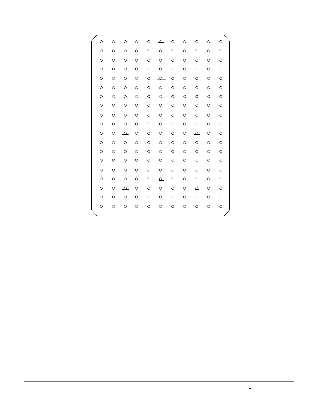
PIN ASSIGNMENT
109876511
A
DQe SA
DQe SA SA SE1
B
DQe DQe SA SA
C
D
E
F
G
H
J
K
L
M
N
P
R
T
U
V
W
DQe SE2 V
DQe
DQe DQe V
DQfDQe
DQf DQf V
DQfDQf
DQf
DQf V
DQfDQf
SBf
SBg NC VSSV
DQgDQg
DQg DQg V
DQgDQg
DQg DQg V
DQh K
DQg
DQh V
DQh
DQh
DQh V
DQh NC SA SA0NCSA
DQh
DQh NC
V
DDQVDD
V
V
DDQ
DDQVDD
V
V
DDQ
DDQVSS
V
SBe
V
SBh
V
DDQ
V
V
DDQ
DDQVDD
V
V
DDQ
DDQ
LBO
V
NCDQh
SA
G
SA
SGW
ADV
ADSC
ADSP
V
SS
V
SS
V
SS
V
SS
V
SS
V
SS
V
SS
NC
SW
SA1
V
DDQ
DDQ
V
SS
V
SS
DD
V
SS
V
SS
DD
V
SS
V
SS
SS
SS
V
SS
SS
V
SS
SS
V
SS
DD
V
SS
V
SS
DD
V
V
DD
SS
V
DDQ
DDQ
SA
NC
NC
SA DQd
SA DQd
SA
DDQ
V
SS
V
SS
V
SS
V
SS
V
SS
V
SS
V
SS
V
SS
V
SS
V
SS
V
SS
V
SS
V
SS
DDQ
SA
SA
SE3
V
DDQ
V
V
DD
DDQ
V
DD
DDQ
V
V
DD
DDQ
V
DD
DDQ
V
V
DDQ
SS
V
SS
VSSNC SBb
V
SS
V
V
DDQ
SS
V
DDQ
DD
V
V
DDQ
DD
V
V
DD
DDQ
V
V
DD
DDQ
FT
V
DDQ
SA
NC DQa
NCNC DQa
141312 15
DQd
DQd
DQd
DQcV
DQc
DQcV
DQc
DQcSBd
DQbSBa
DQb
DQbV
DQb
DQa
DQa
DQa
DQa
DQd
DQd
DQd
DQd
DQc
DQc
DQc
DQc
SBc
DQb
DQb
DQb
DQb
DQb
DQa
DQa
DQa
256K X 72 JEDEC FOUR–CHIP MODULE
TOP VIEW
209 BUMP PBGA
Not to Scale
MOTOROLA FAST SRAM
MCM72FB8ML MCM72PB8ML
3

PIN DESCRIPTIONS
Pin Locations Symbol
E10 ADSC Input Synchronous Address Status Controller: Active low, interrupts any
F10 ADSP Input Synchronous Address Status Processor: Active low, interrupts any
D10 ADV Input Synchronous Address Advance: Increments address count in
(a) R14, T14, T15, U14, U15, V14, V15,
W14, W15
(b) L14, L15, M14, M15, N14, N15, P14,
P15, R15
(c) E14, F14, F15, G14, G15, H14, H15,
J14, J15
(d) A14, A15, B14, B15, C14, C15, D14,
D15, E15
(e) A5, A6, B5, B6, C5, C6, D5, D6, E5
(f) E6, F5, F6, G5, G6, H5, H6, J5, J6
(g) L5, L6, M5, M6, N5, N6, P5, P6, R5
(h) R6, T5, T6, U5, U6, V5, V6, W5, W6
U13 FT Input Flow–Through Input: This pin must remain in steady state (this
B10 G Input Asynchronous Output Enable.
R10 K Input Clock: This signal registers the address, data in, and all control
U7 LBO Input Linear Burst Order Input: This pin must remain in steady state (this
U10, V10 SA1, SA0 Input Synchronous Address Inputs: These pins must be wired to the two
A7, A8, A9, A11, A12, A13, B7, B8, B9,
B11, B12, B13, V8, V9, V11, V12
L13, K14, K15, J13, J7, K5, K6, L7
(a) (b) (c) (d) (e) (f) (g) (h)
A10 SE1 Input Synchronous Chip Enable: Active low to enable chip.
C7 SE2 Input Synchronous Chip Enable: Active high for depth expansion.
C13 SE3 Input Synchronous Chip Enable: Active low for depth expansion.
C10 SGW Input Synchronous Global Write: This signal writes all bytes regardless of
T10 SW Input Synchronous Write: This signal writes only those bytes that have
D8, D12, E8, E12, F8, F12, G8,
G12, N8, N12, P8, P12, R8, R12, T8, T12
C8, C9, C11, C12, D7, D13, E7,
E13, F7, F13, G7, G13, H7, H13,
M7, M13, N7, N13, P7, P13, R7,
R13, T7, T13, U8, U9, U11, U12
Type Description
ongoing burst and latches a new external address. Used to initiate
READ, WRITE, or chip deselect cycle.
ongoing burst and latches a new external address. Used to initiate
READ, WRITE, or chip deselect cycle (exception — chip deselect
does not occur when ADSP
accordance with counter type selected (linear/interleaved).
DQx I/O Synchronous Data I/O: “x” refers to the byte being read or written
SA2 – SA17 Input Synchronous Address Inputs: These inputs are registered and must
SBx Input Synchronous Byte Write Inputs: “x” refers to the byte being written
V
V
DDQ
DD
Supply Core Power Supply.
Supply I/O Power Supply.
(byte a, b, c, d, e, f, g, h).
signal is not registered or latched). It must be tied high or low.
Low — flow–through mode.
High — pipeline mode.
signals except G
signal not registered or latched). It must be tied high or low.
Low — linear burst counter (68K/PowerPC).
High — interleaved burst counter (486/i960/Pentium).
LSBs of the address bus for proper burst operation. These inputs
are registered and must meet setup and hold times.
meet setup and hold times.
(byte a, b, c, d, e, f, g, h). SGW
Negated high–blocks ADSP
asserted.
the status of the SBx
are being used, tie this pin high.
been selected using the byte write SBx
signals SBx
, LBO, and FT.
are being used, tie this pin low.
is asserted and SE1 is high).
overrides SBx.
or deselects chip when ADSC is
and SW signals. If only byte write signals SBx
pins. If only byte write
MCM72FB8ML MCM72PB8ML
4
MOTOROLA FAST SRAM

PIN DESCRIPTIONS (continued)
Pin Locations Symbol Type Description
D9, D11, E9, E11, F9, F11, G9 – G11,
H8 – H12, J8 – J12, K8 – K12, L8 – L12,
M8 – M12, N9 – N11, P9, P11, R9, R11,
T9, T11
K7, K13, P10, V7, V13, W7 – W13 NC — No Connection: There is no connection to the chip.
V
SS
Supply Ground.
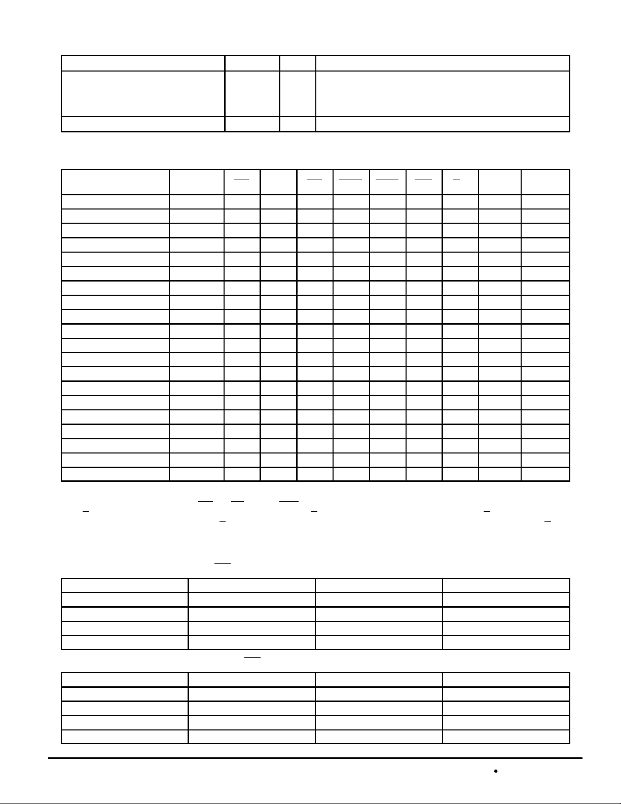
TRUTH TABLE (See Notes 1 through 5)
Address
Next Cycle
Deselect None 1 X X X 0 X X High–Z X
Deselect None 0 X 1 0 X X X High–Z X
Deselect None 0 0 X 0 X X X High–Z X
Deselect None X X 1 1 0 X X High–Z X
Deselect None X 0 X 1 0 X X High–Z X
Begin Read External 0 1 0 0 X X X High–Z X
Begin Read External 0 1 0 1 0 X X High–Z READ
Continue Read Next X X X 1 1 0 1 High–Z READ
Continue Read Next X X X 1 1 0 0 DQ READ
Continue Read Next 1 X X X 1 0 1 High–Z READ
Continue Read Next 1 X X X 1 0 0 DQ READ
Suspend Read Current X X X 1 1 1 1 High–Z READ
Suspend Read Current X X X 1 1 1 0 DQ READ
Suspend Read Current 1 X X X 1 1 1 High–Z READ
Suspend Read Current 1 X X X 1 1 0 DQ READ
Begin Write External 0 1 0 1 0 X X High–Z WRITE
Continue Write Next X X X 1 1 0 X High–Z WRITE
Continue Write Next 1 X X X 1 0 X High–Z WRITE
Suspend Write Current X X X 1 1 1 X High–Z WRITE
Suspend Write Current 1 X X X 1 1 X High–Z WRITE
NOTES:
1. X = Don’t Care. 1 = logic high. 0 = logic low.
2. Write is defined as either 1) any SBx
3. G
is an asynchronous signal and is not sampled by the clock K. G drives the bus immediately (t
4. On write cycles that follow read cycles, G
also remain negated at the completion of the write cycle to ensure proper write data hold times.
5. This read assumes the RAM was previously deselected.
Used
SE1 SE2 SE3 ADSP ADSC ADV G
and SW low or 2) SGW is low.
must be negated prior to the start of the write cycle to ensure proper write data setup times. G must
GLQX
3
DQx Write 2,
) following G going low.
4
5
5
LINEAR BURST ADDRESS TABLE (LBO = V
1st Address (External) 2nd Address (Internal) 3rd Address (Internal) 4th Address (Internal)
X . . . X00 X . . . X01 X . . . X10 X . . . X11
X . . . X01 X . . . X10 X . . . X11 X . . . X00
X . . . X10 X . . . X1 1 X . . . X00 X . . . X01
X . . . X11 X . . . X00 X . . . X01 X . . . X10
INTERLEAVED BURST ADDRESS TABLE (LBO = V
1st Address (External)
X . . . X00 X . . . X01 X . . . X10 X . . . X11
X . . . X01 X . . . X00 X . . . X11 X . . . X10
X . . . X10 X . . . X1 1 X . . . X00 X . . . X01
X . . . X11 X . . . X10 X . . . X01 X . . . X00
2nd Address (Internal) 3rd Address (Internal) 4th Address (Internal)
MOTOROLA FAST SRAM
SS
)
)
DD
MCM72FB8ML MCM72PB8ML
5

WRITE TRUTH TABLE
Cycle Type SGW SW SBa SBb SBc SBd SBe SBf SBg SBh
Read H H X X X X X X X X
Read H L L H H H H H H H
Write Byte a H L L H H H H H H H
Write Byte b H L H L H H H H H H
Write Byte c H L H H L H H H H H
Write Byte d H L H H H L H H H H
Write Byte e H L H H H H L H H H
Write Byte f H L H H H H H L H H
Write Byte g H L H H H H H H L H
Write Byte h H L H H H H H H H L
Write All Bytes H L L L L L L L L L
Write All Bytes L X X X X X X X X X
ABSOLUTE MAXIMUM RATINGS (See Note 1)
Rating Symbol Value Unit Notes
Power Supply Voltage V
I/O Supply Voltage V
Input Voltage Relative to VSS for
Any Pin Except V
Input Voltage (Three–State I/O) V
Output Current (per I/O) I
Package Power Dissipation P
Ambient Temperature T
Die Temperature T
Temperature Under Bias T
Storage Temperature T
NOTES:
1. Permanent device damage may occur if ABSOLUTE MAXIMUM RATINGS are
exceeded. Functional operation should be restricted to RECOMMENDED OPERATING CONDITIONS. Exposure to higher than recommended voltages for extended
periods of time could affect device reliability.
2. This is a steady–state DC parameter that is in effect after the power supply has
achieved its nominal operating level. Power sequencing is not necessary.
3. Power dissipation capability is dependent upon package characteristics and use environment. See Package Thermal Characteristics.
DD
DD
DDQ
Vin, V
out
bias
stg
VSS – 0.5 to + 4.6 V
VSS – 0.5 to V
out
IT
D
A
J
VSS – 0.5 to
VDD + 0.5
VSS – 0.5 to
V
DDQ
0 to 70 °C
– 10 to 85 °C
– 55 to 125 °C
V 2
DD
V 2
+ 0.5
± 20 mA
6.4 W 3
110 °C 3
V 2
This device contains circuitry to protect the
inputs against damage due to high static voltages or electric fields; however, it is advised
that normal precautions be taken to avoid
application of any voltage higher than maximum rated voltages to this high–impedance
circuit.
PACKAGE THERMAL CHARACTERISTICS
Thermal Resistance Symbol Max Unit Notes
Junction to Ambient (@ 200 lfm) Single–Layer Board
Four–Layer Board
Junction to Board (Bottom) R
Junction to Case (Top) R
NOTES:
1. Junction temperature is a function of on–chip power dissipation, package thermal resistance, mounting site (board) temperature, ambient
temperature, air flow, board population, and board thermal resistance.
2. Per SEMI G38–87.
3. Indicates the average thermal resistance between the die and the printed circuit board.
4. Indicates the average thermal resistance between the die and the case top surface via the cold plate method (MIL SPEC–883
Method 1012.1).
MCM72FB8ML MCM72PB8ML
R
θJA
θJB
θJC
19
13
10 °C/W 3
0.3 °C/W 4
°C/W 1, 2
MOTOROLA FAST SRAM
6
 Loading...