

Motorola MCM72F10DG8, MCM72F10DG9, MCM72F10DG12 Datasheet
MOTOROLA
SEMICONDUCTOR TECHNICAL DATA
8MB Synchronous Fast Static
Order this document
by MCM72F10/D
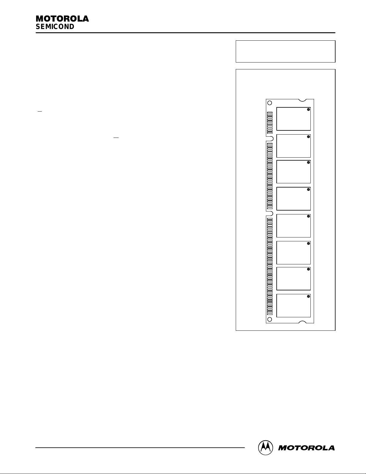
MCM72F10
RAM Module
The MCM72F10 (2MB) is configured as 1M x 72 bits. It is packaged in a
168–pin dual–in–line memory module DIMM. The module uses Motorola’s 3.3 V ,
256K x 18 bit flow–through BurstRAMs.
Address (A), data inputs (DQ, DP), and all control signals except output enable
) are clock (K) controlled through positive–edge–triggered noninverting
(G
registers.
Write cycles are internally self–timed and initiated by the rising edge of the
clock (K) input. This feature provides increased timing flexibility for incoming
signals. Synchronous byte write (W
both bytes.
• Single 3.3 V + 10%, – 5% Power Supply
• Plug and Pin Compatibility with 1MB, 2MB, and 4MB
• Multiple Clock Pins for Reduced Loading
• All Inputs and Outputs are L VTTL Compatible
• Byte Write Capability
• Fast SRAM Access Times: 8/9/12 ns
• High Quality Multi–Layer FR4 PWB With Separate Power and Ground
Planes
• Amp Connector, Part Number: 390064–4
• 168–Pin DIMM Module
) allows writes to either individual bytes or to
168–LEAD DIMM
CASE TBD
TOP VIEW
1
11
40
41
REV 1
11/26/97
Motorola, Inc. 1997
MOTOROLA FAST SRAM
84
MCM72F10
1
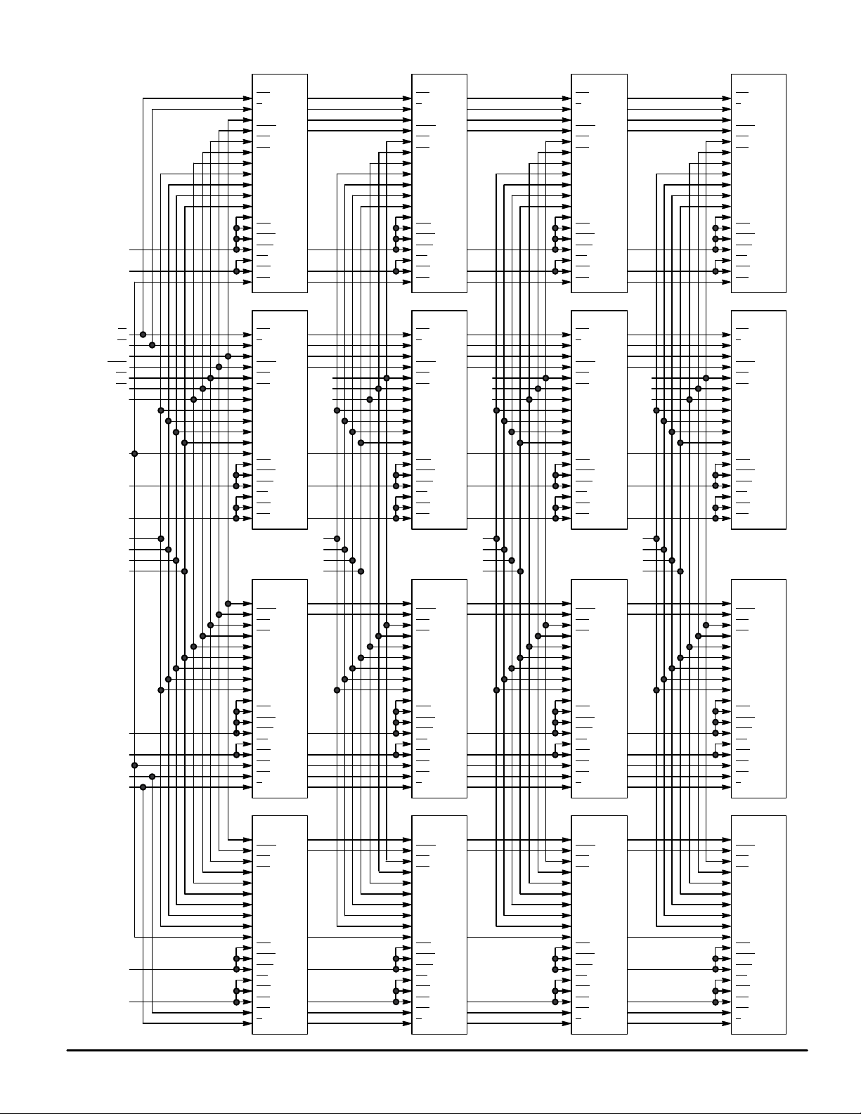
BLOCK DIAGRAM
256K x 18
SE1
G
A0 – A17
ADSC
SBa
SBb
K
DQa0 – DQa7
DQa8
DQb0 – DQb7
DQb8
SE2
ADV
V
DD
V
SS
ADSP
SGW
SW
LBO
SE3
256K x 18
SE1
G
A0 – A17
ADSC
SBa
SBb
K
DQa0 – DQa7
DQa8
DQb0 – DQb7
DQb8
SE2
ADV
ADSP
SGW
SW
LBO
SE3
256K x 18
SE1
G
A0 – A17
ADSC
SBa
SBb
K
DQa0 – DQa7
DQa8
DQb0 – DQb7
DQb8
SE2
ADV
ADSP
SGW
SW
LBO
SE3
256K x 18
SE1
G
A0 – A17
ADSC
SBa
SBb
K
DQa0 – DQa7
DQa8
DQb0 – DQb7
DQb8
SE2
ADV
ADSP
SGW
SW
LBO
SE3
E0
G0
A0 – A17
ADSP
W0
W1
KO
A18
V
DD
V
SS
DQ0 – DQ7
DP0
DQ8 – DQ15
DP1
V
DD
V
SS
E1
G1
256K x 18
SE1
G
A0 – A17
ADSC
SBa
SBb
K
DQa0 – DQa7
DQa8
DQb0 – DQb7
DQb8
SE2
ADV
ADSP
SGW
SW
LBO
SE3
DQ16 – DQ23
DQ24 – DQ31
256K x 18
A0 – A17
ADSC
SBa
SBb
K
DQb8
DQb0 – DQb7
DQa8
DQa0 – DQa7
SE2
ADV
ADSP
SGW
SW
LBO
SE3
SE1
G
DP2
DP3
W2
W3
256K x 18
SE1
G
A0 – A17
ADSC
SBa
K1
SBb
K
DQa0 – DQa7
DQa8
DQb0 – DQb7
DQb8
SE2
ADV
ADSP
SGW
SW
LBO
SE3
DQ32 – DQ39
DQ40 – DQ47
DP4
DP5
W4
W5
K2
256K x 18
SE1
G
A0 – A17
ADSC
SBa
SBb
K
DQa0 – DQa7
DQa8
DQb0 – DQb7
DQb8
SE2
ADV
ADSP
SGW
SW
LBO
SE3
DQ48 – DQ55
DQ56 – DQ63
DP6
DP7
W6
W7
256K x 18
SE1
G
A0 – A17
ADSC
SBa
K3
SBb
K
DQa0 – DQa7
DQa8
DQb0 – DQb7
DQb8
SE2
ADV
ADSP
SGW
SW
LBO
SE3
256K x 18 256K x 18 256K x 18
A0 – A17
ADSC
SBa
SBb
K
DQb8
DQb0 – DQb7
DQa8
DQa0 – DQa7
SE2
ADV
ADSP
SGW
SW
LBO
SE3
SE1
G
A0 – A17
ADSC
SBa
SBb
K
DQb8
DQb0 – DQb7
DQa8
DQa0 – DQa7
SE2
ADV
ADSP
SGW
SW
LBO
SE3
SE1
G
A0 – A17
ADSC
SBa
SBb
K
DQb8
DQb0 – DQb7
DQa8
DQa0 – DQa7
SE2
ADV
ADSP
SGW
SW
LBO
SE3
SE1
G
V
DD
V
SS
MCM72F10
2
256K x 18
A0 – A17
ADSC
SBa
SBb
K
DQb8
DQb0 – DQb7
DQa8
DQa0 – DQa7
SE2
ADV
ADSP
SGW
SW
LBO
SE3
SE1
G
256K x 18 256K x 18 256K x 18
A0 – A17
ADSC
SBa
SBb
K
DQb8
DQb0 – DQb7
DQa8
DQa0 – DQa7
SE2
ADV
ADSP
SGW
SW
LBO
SE3
SE1
G
A0 – A17
ADSC
SBa
SBb
K
DQb8
DQb0 – DQb7
DQa8
DQa0 – DQa7
SE2
ADV
ADSP
SGW
SW
LBO
SE3
SE1
G
A0 – A17
ADSC
SBa
SBb
K
DQb8
DQb0 – DQb7
DQa8
DQa0 – DQa7
SE2
ADV
ADSP
SGW
SW
LBO
SE3
SE1
G
MOTOROLA FAST SRAM
V
SS
DQ63
DQ62
V
DD
DQ60
DQ58
V
SS
DQ56
DQ55
V
SS
1
2
3
4
5
6
7
8
9
10
85
86
87
88
89
90
91
92
93
94
PIN ASSIGNMENT
168–LEAD DIMM
TOP VIEW
V
SS
DP7
DQ61
V
SS
DQ59
DQ57
V
SS
DP6
DQ54
V
DD
DQ53
DQ51
V
SS
DQ49
DP5
V
DD
DQ46
DQ44
V
SS
DQ42
DQ40
V
SS
DQ39
DQ37
V
SS
DQ35
DQ33
V
SS
K3
V
SS
DP3
DQ30
V
DD
DQ28
DQ26
V
SS
DQ24
DQ23
V
SS
DQ21
11
12
13
14
15
16
17
18
19
20
21
22
23
24
25
26
27
28
29
30
31
32
33
34
35
36
37
38
39
40
95
96
97
98
99
100
101
102
103
104
105
106
107
108
109
110
111
112
113
114
115
116
117
118
119
120
121
122
123
124
DQ52
DQ50
V
SS
DQ48
DQ47
V
SS
DQ45
DQ43
V
SS
DQ41
DP4
V
DD
DQ38
DQ36
V
SS
DQ34
DQ32
V
SS
K2
V
SS
DQ31
DQ29
V
SS
DQ27
DQ25
V
SS
DP2
DQ22
V
DD
DQ20
DQ19
V
SS
DQ17
DP1
V
DD
DQ14
DQ12
V
SS
DQ10
DQ8
V
SS
DQ7
DQ5
V
SS
DQ3
DQ1
V
DD
NC
A18
V
SS
A16
A14
V
SS
A12
A10
V
SS
A8
A6
V
DD
A4
A2
A0
V
SS
K1
V
SS
W7
W5
V
SS
W3
W1
V
SS
G1
E1
V
SS
41
42
43
44
45
46
47
48
49
50
51
52
53
54
55
56
57
58
59
60
61
62
63
64
65
66
67
68
69
70
71
72
73
74
75
76
77
78
79
80
81
82
83
84
125
126
127
128
129
130
131
132
133
134
135
136
137
138
139
140
141
142
143
144
145
146
147
148
149
150
151
152
153
154
155
156
157
158
159
160
161
162
163
164
165
166
167
168
DQ18
V
SS
DQ16
DQ15
V
SS
DQ13
DQ11
V
SS
DQ9
DP0
V
DD
DQ6
DQ4
V
SS
DQ2
DQ0
V
SS
NC
A17
V
SS
A15
A13
V
DD
A11
A9
V
SS
A7
A5
V
SS
A3
A1
ADSP
V
SS
K0
V
SS
W6
W4
V
SS
W2
W0
V
DD
G0
E0
V
SS
MOTOROLA FAST SRAM
MCM72F10
3
PIN DESCRIPTIONS
Pin Locations Symbol Type Description
59, 61, 62, 64, 65, 67, 68, 70,
71, 72, 143, 145, 146, 148,
149, 151, 152, 154, 155
156 ADSP Input Synchronous Addresss Status Controller: Initiates read, write, or chip
15, 31, 44, 86, 92, 105, 121,
134
2, 3, 5, 6, 8, 9, 11, 12, 14, 17,
18, 20, 21, 23, 24, 26, 27, 32,
34, 35, 37, 38, 40, 41, 43, 46,
47, 49, 50, 52, 53, 55, 56, 87,
89, 90, 93, 95, 96, 98, 99,
101, 102, 104, 107, 108, 110,
111, 115, 1 16, 118, 119, 122,
124, 125, 127, 128, 130, 131,
133, 136, 137, 139, 140
83, 167 E0, E1 Input Synchronous Chip Enable: Active low to enable chip. Negated high —
82, 166 G0, G1 Input Asynchronous Output Enable Input:
29, 74, 113, 158 K0 – K3 Input Clock: This signal registers the address, data in, and all control signals
76, 77, 79, 80, 160, 161, 163,
164
4, 16, 33, 45, 57, 69, 94, 106,
123, 135, 147, 165
1, 7, 10, 13, 19, 22, 25, 28,
30, 36, 39, 42, 48, 51, 54, 60,
63, 66, 73, 75, 78, 81, 84, 85,
88, 91, 97, 100, 103, 109,
112, 114, 117, 120, 126, 129,
132, 138, 141, 144, 150, 153,
157, 159, 162, 168
58, 142 NC No Connection: There is no connection to the chip.
A0 – A18 Input Synchronous Address Inputs: These inputs are registered and must meet
DP0 – DP7 Synchronous Parity Data Inputs/Outputs.
DQ0 – DQ63 I/O Synchronous Data Inputs/Outputs.
W0 – W7 Input Synchronous Byte Write Inputs: x refers to the byte being written (byte a,
V
DD
V
SS
Supply Power Supply: 3.3 V + 10%, – 5%. Must be connected on all modules.
Supply Ground.
setup and hold times.
deselect cycle.
blocks ADSP
Low — enables output buffer.
High — DQx pins are high impedance.
except G
b).
or deselects chip when ADSC is asserted.
and LBO.
DATA RAM MCM69F618A SYNCHRONOUS TRUTH TABLE (See Notes 1, 2, 3, and 4)
Next Cycle Address Used E ADSP G DQx WRITE
Deselect None 1 0 X High–Z X
Begin Read External Address 0 0 0 DQ Read
Read Current X 1 1 High–Z Read
Read Current X 1 0 DQ Read
Begin Write External 0 0 X High–Z Write
Write Current X 1 X High–Z Write
NOTES:
1. X = don’t care, 1 = logic high, 0 = logic low.
2. Write is defined as any Wx
3. G
is an asynchronous signal and is not sampled by the clock K. G drives the bus immediately (t
4. On write cycles that follow read cycles, G
also remain negated at the completion of the write cycle to ensure proper write data hold times.
low.
must be negated prior to the start of the write cycle to ensure proper write data setup times. G must
MCM72F10
4
) following G going low.
GLQX
MOTOROLA FAST SRAM
 Loading...