

Motorola MCM72BA64SG66, MCM72BA64SG50, MCM72BA32SG66, MCM72BA32SG60, MCM72BA64SG60 Datasheet
...
MCM72BA32•MCM72BA64
1
MOTOROLA FAST SRAM
256KB and 512KB BurstRAM
Secondary Cache Module for
Pentium
The MCM72BA32SG and MCM72BA64SG are designed to provide a burstable, high performance, 256K/512K L2 cache for the Pentium microprocessor.
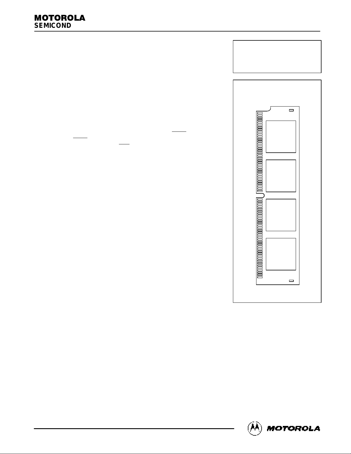
The modules are configured as 32K x 72 and 64K x 72 bits in a 136 pin dual readout single inline memory module (DIMM). The module uses four of Motorola’s
MCM67B518 or MCM67B618 BiCMOS BurstRAMs.
Bursts can be initiated with either address status processor (ADSP
) or address
status controller (ADSC
). Subsequent burst addresses are generated internal to
the BurstRAM by the burst advance (ADV
) input pin.
Write cycles are internally self timed and are initiated by the rising edge of the
clock (K) input. Eight write enables are provided for byte write control.
The cache family is designed to interface with popular Pentium cache controllers with on board TAG.
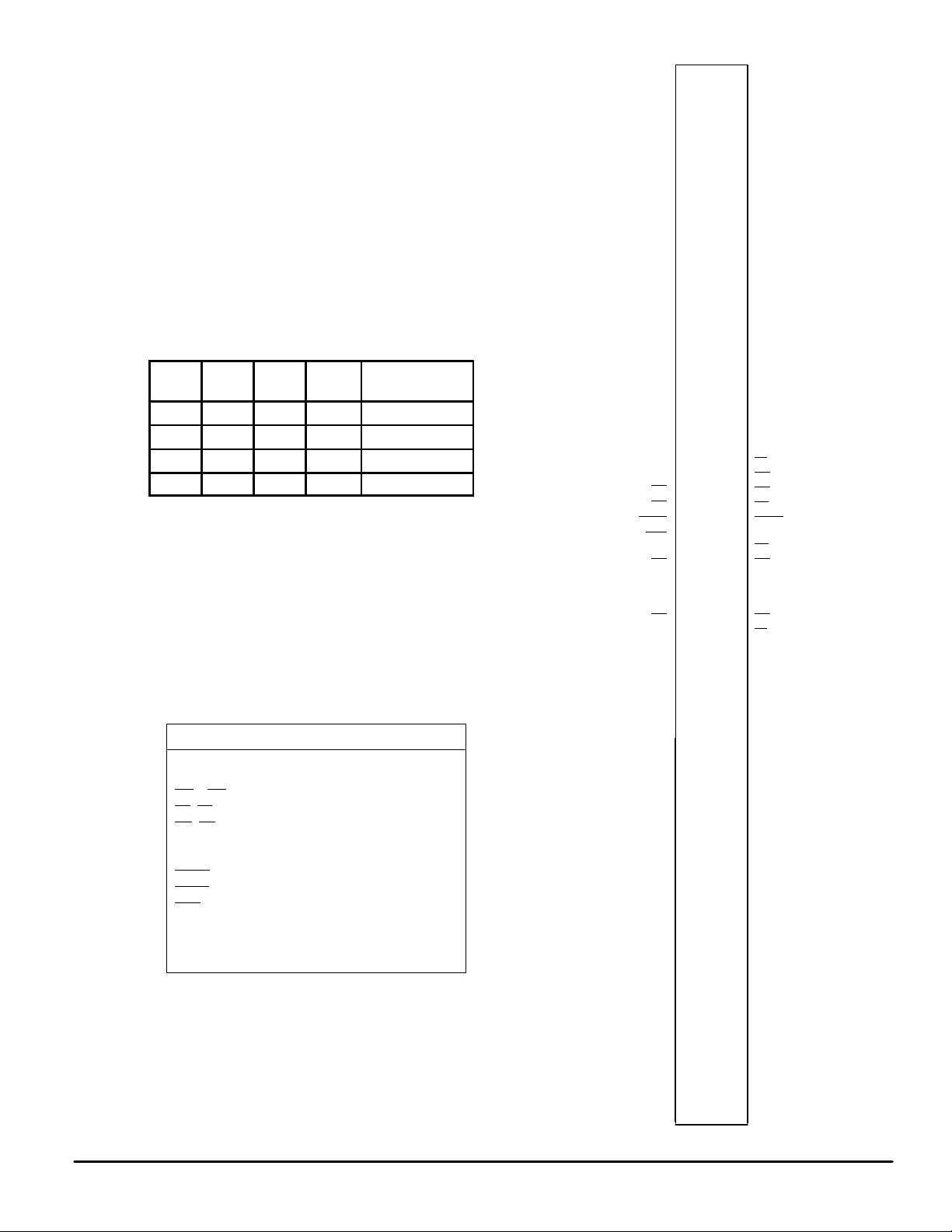
PD0 – PD2 are reserved for density and speed identification.
• Pentium–style Burst Counter on Board
• Dual Readout SIMM for Circuit Density
• Single 5 V ± 5% Power Supply
• All Inputs and Outputs are TTL Compatible
• Three State Outputs
• Byte Parity
• Byte Write Capability
• Fast Module Clock Rates: 66 MHz, 60 MHz, 50MHz
• Decoupling Capacitors for each Fast Static RAM
• High Quality Multi–Layer FR4 PWB With Separate Power and Ground Planes
• I/Os are 3.3 V Compatible
BurstRAM is a trademark of Motorola.
Pentium is a trademark of Intel Corp.
Order this document
by MCM72BA32/D
MOTOROLA
SEMICONDUCTOR TECHNICAL DATA
MCM72BA32
MCM72BA64
68
35
34
1
136–LEAD DIMM
CASE 1104–01
TOP VIEW
REV 2
5/95
Motorola, Inc. 1995
PIN ASSIGNMENT
136–LEAD DIMM
TOP VIEW
PD0
PD1
DQ0
DQ1
V
CC
DQ4
DQ6
DQP0
DQ8
DQ10
V
SS
K0
V
SS
DQ14
V
CC
DQ16
DQ17
DQ19
DQ21
V
CC
DQP2
DQ24
DQ26
DQ28
V
SS
DQ31
DQP3
69
70
71
72
73
74
75
76
77
78
79
80
81
82
83
84
85
86
87
88
89
90
91
92
93
94
95
96
97
98
99
100
101
102
1
2
3
4
5
6
7
8
9
10
11
12
13
14
15
16
17
18
19
20
21
22
23
24
25
26
27
28
29
30
31
32
33
34
V
SS
PD2
V
CC
DQ2
DQ3
DQ5
DQ7
V
SS
DQ9
DQ11
DQ12
V
SS
DQ13
DQ15
DQP1
V
SS
DQ18
DQ20
DQ22
DQ23
V
SS
DQ25
DQ27
DQ29
DQ30
103
104
105
106
107
108
109
110
111
112
113
114
115
116
117
118
119
120
121
122
123
124
125
126
127
128
129
130
131
132
133
134
135
136
35
36
37
38
39
40
41
42
43
44
45
46
47
48
49
50
51
52
53
54
55
56
57
58
59
60
61
62
63
64
65
66
67
68
W6
DQ32
DQ33
V
SS
DQ36
DQ38
DQ39
DQ40
V
CC
DQ43
DQ45
DQ46
DQP5
V
SS
K1
V
SS
DQ52
DQ53
DQ55
DQP6
V
CC
DQ58
DQ60
DQ62
DQP7
A0
A2
A4
A6
A8
A10
A12
A14
V
SS
W7
E1
DQ34
DQ35
DQ37
V
CC
DQP4
DQ41
DQ42
DQ44
V
SS
DQ47
DQ48
DQ49
V
SS
DQ50
DQ51
DQ54
DQ56
V
SS
DQ57
DQ59
DQ61
DQ63
V
CC
A1
A3
A5
A7
NC
A9
A11
A13
A15*
W0
W2
ADSP
ADV
E0
W1
W3
G0
ADSC
W4
G1
W5
V
CC
V
SS
V
SS
V
SS
PIN NAMES
A0 – A15 Address Inputs. . . . . . . . . . . . . . . . . . . . . .
K0, K1 Clock. . . . . . . . . . . . . . . . . . . . . . . . . . . . . . . .
W0
– W7 Byte Write. . . . . . . . . . . . . . . . . . . . . . . . . .
E0
, E1 Module Enable. . . . . . . . . . . . . . . . . . . . . . . .
G0
, G1 Module Output Enable. . . . . . . . . . . . . . . . .
DQ0 – DQ63 Cache Data Input/Output. . . . . . . . . .
DQP0 – DQP7 Data Parity Input/Output. . . . . . . . .
ADSC
Controller Address Status. . . . . . . . . . . . . .
ADSP
Processor Address Status. . . . . . . . . . . . . . .
ADV
Burst Advance. . . . . . . . . . . . . . . . . . . . . . . . . .
PD0 – PD2 Presence Detect. . . . . . . . . . . . . . . . . .
V
CC
+ 5 V Power Supply. . . . . . . . . . . . . . . . . . . . . .
V
SS
Ground. . . . . . . . . . . . . . . . . . . . . . . . . . . . . . . .
* This pin on the MCM72BA32 is a No Connect (NC)
MCM72BA32•MCM72BA64
2
MOTOROLA FAST SRAM
PD2 PD1 PD0
Cache
Size
Module
V
SS
NC NC 512KB 72BA64SG66/60
V
SS
NC V
SS
512KB 72BA64SG50
V
SS
V
SS
NC 256KB 72BA32SG66/60
V
SS
V
SS
V
SS
256KB 72BA32SG50
MCM72BA32•MCM72BA64
3
MOTOROLA FAST SRAM
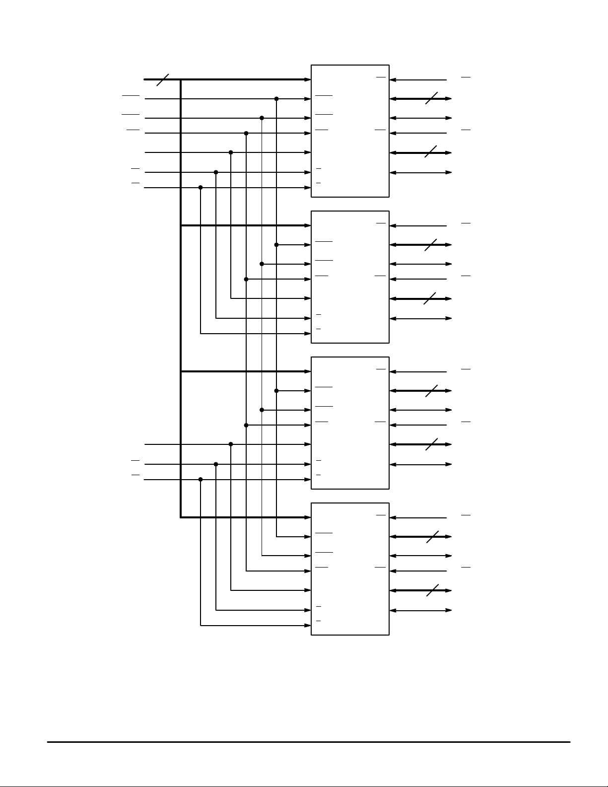
64K x 72 BurstRAM MEMORY MODULE BLOCK DIAGRAM
LW
MCM67B618
A0 – A15
ADV
K
G
E
DQ0 – DQ7
A0 – A15
E0
16
K1
E1
G1
DQ8
UW
ADSP
ADSC
DQ9 – DQ16
DQ17
ADV
ADSP
ADSC
K0
G0
DQ0 – DQ7
DQP0
DQ8 – DQ15
DQP1
W0
W1
8
8
LW
MCM67B618
A0 – A15
ADV
K
G
E
DQ0 – DQ7
DQ8
UW
ADSP
ADSC
DQ9 – DQ16
DQ17
DQ16 – DQ23
DQP2
DQ24 – DQ31
DQP3
W2
W3
8
8
LW
MCM67B618
A0 – A15
ADV
K
G
E
DQ0 – DQ7
DQ8
UW
ADSP
ADSC
DQ9 – DQ16
DQ17
DQ32 – DQ39
DQP4
DQ40 – DQ47
DQP5
W4
W5
8
8
LW
MCM67B618
A0 – A15
ADV
K
G
E
DQ0 – DQ7
DQ8
UW
ADSP
ADSC
DQ9 – DQ16
DQ17
DQ48 – DQ55
DQP6
DQ56 – DQ63
DQP7
W6
W7
8
8
MCM72BA32•MCM72BA64
4
MOTOROLA FAST SRAM
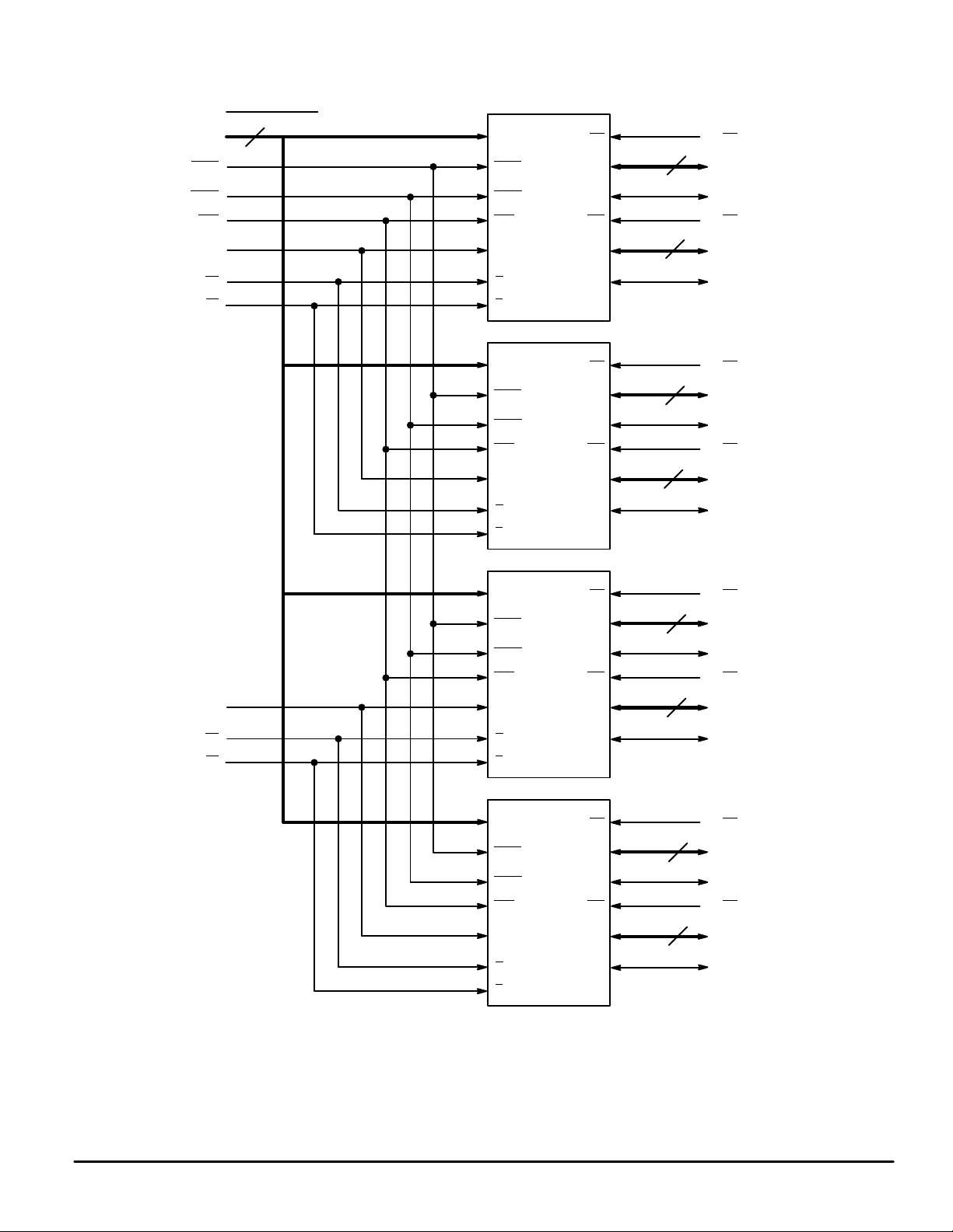
32K x 72 BurstRAM MEMORY MODULE BLOCK DIAGRAM
LW
MCM67B518
A0 – A14
ADV
K
G
E
DQ0 – DQ7
A0 – A14
E0
15
K1
E1
G1
DQ8
UW
ADSP
ADSC
DQ9 – DQ16
DQ17
ADV
ADSP
ADSC
K0
G0
DQ0 – DQ7
DQP0
DQ8 – DQ15
DQP1
W0
W1
8
8
LW
MCM67B518
A0 – A14
ADV
K
G
E
DQ0 – DQ7
DQ8
UW
ADSP
ADSC
DQ9 – DQ16
DQ17
DQ16 – DQ23
DQP2
DQ24 – DQ31
DQP3
W2
W3
8
8
LW
MCM67B518
A0 – A14
ADV
K
G
E
DQ0 – DQ7
DQ8
UW
ADSP
ADSC
DQ9 – DQ16
DQ17
DQ32 – DQ39
DQP4
DQ40 – DQ47
DQP5
W4
W5
8
8
LW
MCM67B518
A0 – A14
ADV
K
G
E
DQ0 – DQ7
DQ8
UW
ADSP
ADSC
DQ9 – DQ16
DQ17
DQ48 – DQ55
DQP6
DQ56 – DQ63
DQP7
W6
W7
8
8
A15 NC
MCM72BA32•MCM72BA64
5
MOTOROLA FAST SRAM
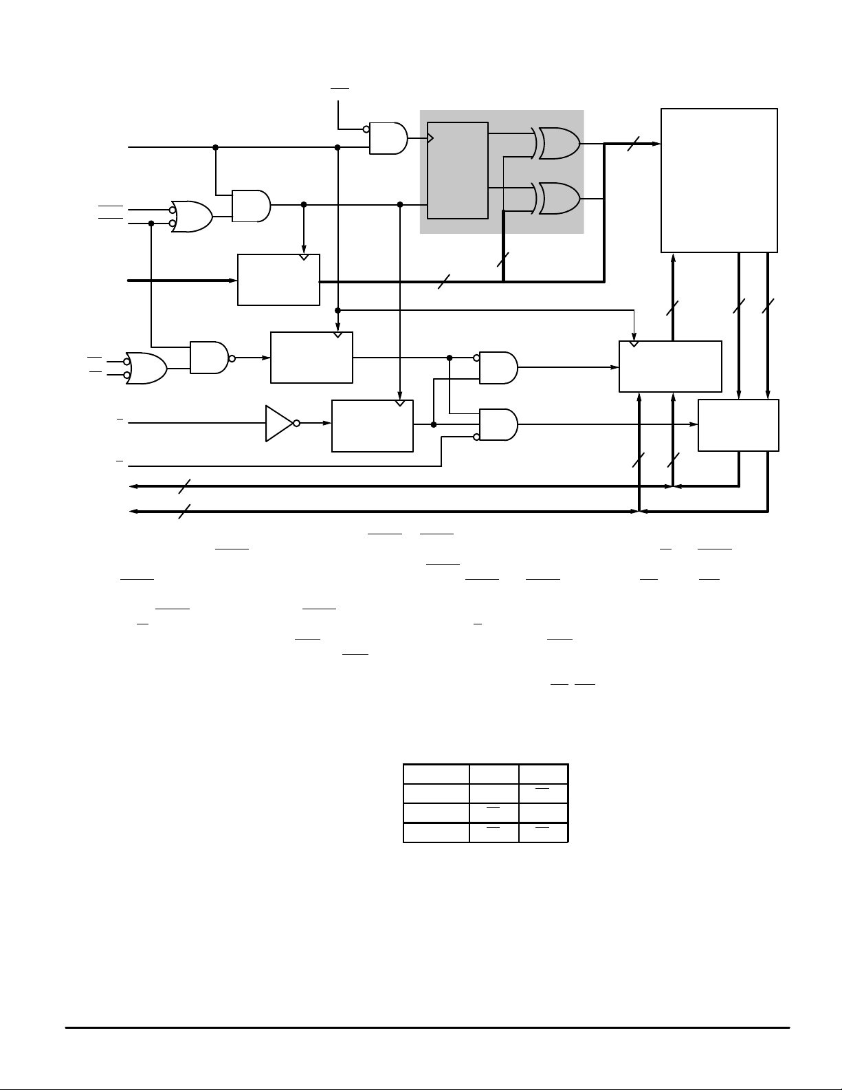
MCM67B618 BLOCK DIAGRAM (See Note)
BINARY
COUNTER
DQ0 – DQ8
CLR
Q0
Q1
A0
A1
K
ADSC
ADSP
A0 – A15
E
G
ADDRESS
REGISTER
WRITE
REGISTER
ENABLE
REGISTER
DATA–IN
REGISTERS
OUTPUT
BUFFER
64K
×
18
MEMORY
ARRAY
ADV
BURST LOGIC
INTERNAL
ADDRESS
A0
′
A1
′
16
9
18
16
2
A2 – A15
A1 – A0
DQ9 – DQ17
9
9 9
9
9
UW
LW
NOTE: All registers are positive–edge triggered. The ADSC or ADSP signals control the duration of the burst and the start of the
next burst. When ADSP
is sampled low, any ongoing burst is interrupted and a read (independent of W and ADSC) is per-
formed using the new external address. Alternatively , an ADSP
–initiated two cycle WRITE can be performed by asserting
ADSP
and a valid address on the first cycle, then negating both ADSP and ADSC and asserting L W and/or UW with valid
data on the second cycle (see Single Write Cycle in WRITE CYCLES timing diagram).
When ADSC
is sampled low (and ADSP is sampled high), any ongoing burst is interrupted and a read or write (dependent
on W
) is performed using the new external address. Chip enable (E) is sampled only when a new base address is loaded.
After the first cycle of the burst, ADV
controls subsequent burst cycles. When ADV is sampled low, the internal address
is advanced prior to the operation. When ADV
is sampled high, the internal address is not advanced, thus inserting a wait
state into the burst sequence accesses. Upon completion of a burst, the address will wrap around to its initial state. See
BURST SEQUENCE TABLE. Write refers to either or both byte write enables (LW
, UW).
BURST SEQUENCE TABLE (See Note)
External Address A15 – A2 A1 A0
1st Burst Address A15 – A2 A1 A0
2nd Burst Address A15 – A2 A1 A0
3rd Burst Address A15 – A2 A1 A0
NOTE: The burst wraps around to its initial state upon completion.
 Loading...