

Motorola MCM69T618TQ5R, MCM69T618TQ5 Datasheet
MOTOROLA
SEMICONDUCTOR TECHNICAL DATA
64K x 18 Bit Synchronous
Pipelined Cache Tag RAM
The MCM69T618 is a 1M–bit synchronous fast static RAM with integrated tag
compare function. It is designed to address tag RAM for 512KB, 1MB, or 2MB
secondary cache as well as to be used as a data RAM for 512KB caches. This
device is organized as 64K words of 18 bits each. It integrates input registers,
output registers, tag comparators, and high speed SRAM onto a single monolithic circuit for reduced parts count in cache tag RAM applications. Synchronous
design allows precise cycle control with the use of an external clock (K). BiCMOS
circuitry reduces the overall power consumption of the integrated functions for
greater reliability .
Addresses (SA), data inputs (DQ), write enable (SW
and SE1
isters. Data enable (DE
(G) and match output enable (MG) are asynchronous.
clock (K) input. This feature eliminates complex off–chip write pulse generation
and provides increased timing flexibility for incoming signals.
edge–triggered output register and then released to the output buffers at the next
rising edge of clock (K).
can be loaded into the input register. The comparator compares the read data
with the registered input data, and a match signal is generated. The match output
is also stored by an output register and released to the match output buffer at the
next rising edge of clock (K).
outputs are L VTTL compatible.
• MCM69T618–5 = 5 ns Clock–to–Match / 10 ns cycle
• Single 3.3 V + 10%, – 5% Power Supply
• Pipelined Data Comparator
• Pipelined Chip Enable and Write Enable for Data (DQ) Output Enable Path
• 64K x 18 Organization Supports Up to 2MB Cache
• Synchronous Data Input Register Load Enable (DE
• Internally Self–Timed Write Cycle
• Asynchronous Data I/O Output Enable (G
• Asynchronous Match Output Enable (MG
• 100–Pin TQFP Package
) are all controlled through positive–edge–triggered noninverting reg-
) is sampled on the rising clock edge while output enable
Write cycles are internally self–timed and initiated by the rising edge of the
For read cycles, pipelined SRAM output data is temporarily stored by an
Compare cycles begin as read cycles with output disabled, so compare data
The MCM69T618 operates from a single 3.3 V power supply and all inputs and
)
)
), and chip enable (SE0
)
Order this document
by MCM69T618/D
MCM69T618
TQ PACKAGE
TQFP
CASE 983A–01
REV 5
12/23/97
Motorola, Inc. 1997
MOTOROLA FAST SRAM
MCM69T618
1
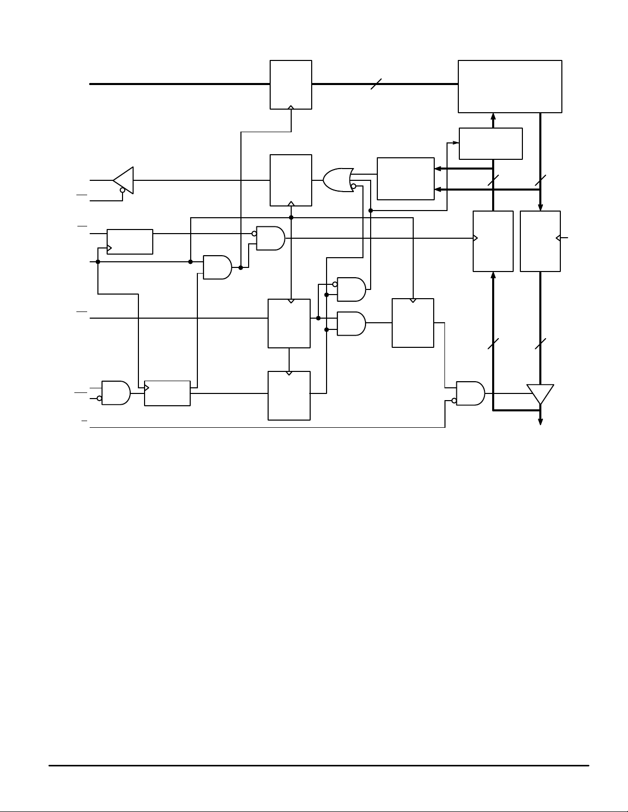
FUNCTIONAL BLOCK DIAGRAM
SA
MATCH
MG
DE
SW
REGISTER
REGISTER
LATCH
K
REGISTER
16
COMPARE
REGISTER
64K x 18 ARRAY
WRITE
DRIVER
18
DATA–IN
REGISTER
18 18
18
DATA–OUT
REGISTER
K
SE0
SE1
LATCH
G
REGISTER
DQ1–DQ18
MCM69T618
2
MOTOROLA FAST SRAM
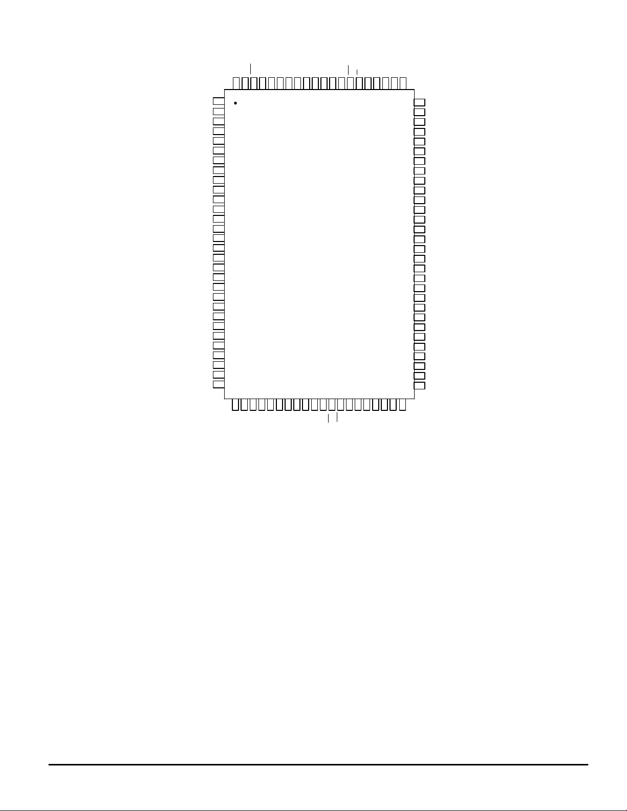
PIN ASSIGNMENT
NC
NC
NC
V
CC
V
SS
NC
NC
DQ10
DQ11
V
SS
V
CC
DQ12
DQ13
NC
V
CC
NC
V
SS
DQ14
DQ15
V
CC
V
SS
DQ16
DQ17
DQ18
NC
V
SS
V
CC
NC
NC
NC
1
2
3
4
5
6
7
8
9
10
11
12
13
14
15
16
17
18
19
20
21
22
23
24
25
26
27
28
29
30
31 3233
SASASE1
CC
SE0
NC
NC
NCNCNC
94 93979695 89889291 90 8685871009998 81828384
3738343536 42433940 41 454644
K
VSSV
NC
SW
NC
G
NC
NC
SA
SA
SA
80
79
NC
78
NC
V
77
CC
76
V
SS
NC
75
DQ9
74
73
DQ8
72
DQ7
71
V
SS
70
V
CC
69
DQ6
68
DQ5
V
67
SS
NC
66
V
65
CC
NC
64
DQ4
63
DQ3
62
V
61
CC
V
60
SS
DQ2
59
58
DQ1
NC
57
NC
56
V
55
SS
V
54
CC
NC
53
52
NC
NC
51
50494847
SASASA
NC
SA
SA
SA
SS
V
TOP VIEW
100–PIN TQFP
V
MATCH
SS
CC
V
DE
MG
SASASA
SA
SA
NC
NC
Not to Scale
MOTOROLA FAST SRAM
MCM69T618
3
 Loading...