

Motorola MCM69D618TQ8, MCM69D618TQ8R, MCM69D618TQ6, MCM69D618TQ6R Datasheet
MOTOROLA
SEMICONDUCTOR TECHNICAL DATA
Order this document
by MCM69D618/D
64K x 18 Bit Synchronous
Dual I/O, Dual Address SRAM
The MCM69D618 is a 1M–bit static random access memory , organized as 64K
words of 18 bits. It features common data input and data output buffers and
incorporates input and output registers on–board with high speed SRAM.
The MCM69D618 allows the user to concurrently perform reads, writes, or
pass–through cycles in combination on the two data ports. The two address ports
(AX, AY) determine the read or write locations for their respective data ports
(DQX, DQY).
The synchronous design allows for precise cycle control with the use of an
external single clock (K). All signal pins except output enables (GX
registered on the rising edge of clock (K).
The pass–through feature allows data to be passed from one port to the other,
in either direction. The PTX
port Y. The PTY
operation takes precedence over a read operation.
For the case when AX and A Y are the same, certain protocols are followed. If
both ports are read, the reads occur normally . If one port is written and the other
is read, the read from the array will occur before the data is written. If both ports
are written, only the data on DQY will be written to the array .
• Single 3.3 V ± 5% Power Supply
• Fast Access Times: 6/8 ns Max
• Throughput of 1.49 Gigabits/Second
• Single Clock Operation
• Address, Data Input, E1
On–Chip
• 83 MHz Maximum Clock Frequency
• Self Timed Write
• Two Bi–Directional Data Buses
• Can be Configured as Separate I/O
• Pass–Through Feature
• Asynchronous Output Enables (GX
• L VTTL Compatible I/O
• Concurrent Reads and Writes
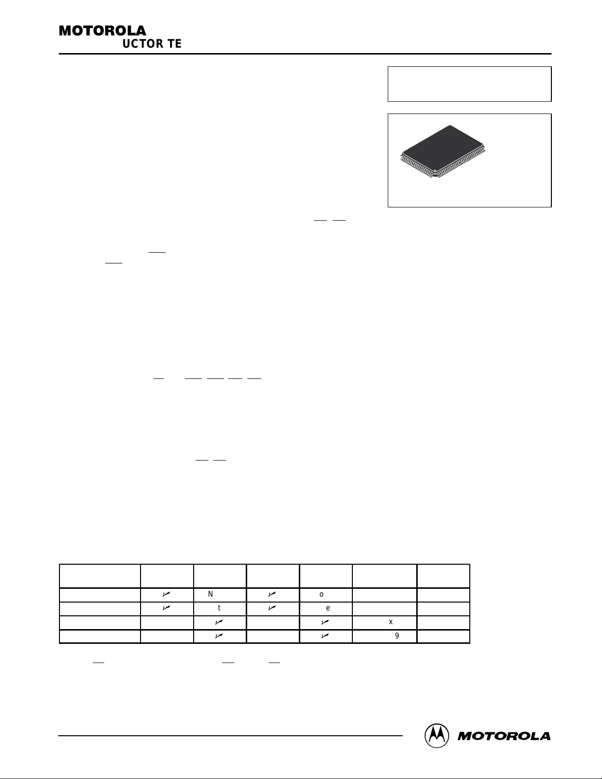
• 100–Pin TQFP Package
Suggested Applications
— A TM — Ethernet Switches — Routers
— Cell/Frame Buffers — SNA Switches — Shared Memory
will likewise pass data from port Y to port X. A pass–through
input must be asserted to pass data from port X to
, E2, PTX, PTY, WX, WY, and Data Output Registers
, GY)
, GY) are
MCM69D618
TQ PACKAGE
100 LEAD TQFP
CASE 983A–01
Product Family Configurations
Part
Number
MCM69D536
MCM69D618
MCM67Q709A
MCM67Q909
NOTES:
1. Tie AX and AY address ports together for the part to function as a single address part.
2. Tie GX
REV 5
1/16/98
Motorola, Inc. 1998
MOTOROLA FAST SRAM
high for DQX to be inputs and tie WY high and GY low for DQY to be outputs.
Dual
Address
n
n
Single
Address
Note 1
Note 1
n n
n n
Dual
I/O
n
n
Separate
I/O
Note 2 32K x 36 3.3 V
Note 2 64K x 18 3.3 V
Configuration V
128K x 9 5.0 V
512K x 9 5.0 V
DD
MCM69D618
1
BLOCK DIAGRAM
AX
WX
PTX
E1
E2
GX
16
K
ENABLE
REG 1
ENABLE
REG 2
ADDRESS
REGISTER
WRITE X
REGISTER
PTX
REGISTER
WRITE
DRIVER
DATA IN
REGISTER
64K x 18 ARRAY
SENSE
AMPS
PASS–THROUGH
OUTPUT
REGISTER
DQX
SENSE
AMPS
OUTPUT
REGISTER
DQY
WRITE
DRIVER
DATA IN
REGISTER
ADDRESS
REGISTER
WRITE Y
REGISTER
PTY
REGISTER
K
16
AY
WY
PTY
GY
MCM69D618
2
MOTOROLA FAST SRAM
PIN ASSIGNMENT
V
DD
V
SS
DQX9
DQY9
DQX10
DQY10
V
DD
V
SS
DQX11
DQY11
DQX12
DQY12
V
DD
V
SS
DQY13
DQX13
DQY14
DQX14
V
DD
V
SS
DQY15
DQX15
DQY16
DQX16
V
DD
V
SS
DQY17
DQX17
AY5
AX5
AX6
1
2
3
4
5
6
7
8
9
10
11
12
13
14
15
16
17
18
19
20
21
22
23
24
25
26
27
28
29
30
31 32 33
AY6
AX7
DD
AY7
VSSV
K
94 9397 96 95 89 8892 91 90 86 8587100 99 98 81828384
37 3834 35 36 42 4339 40 41 45 4644
GY
GX
E2
E1
WY
WX
PTY
PTX
AX8
AY8
AX9
AY9
AX15
79
77
76
72
71
70
69
68
67
66
65
64
63
62
61
60
59
58
57
56
55
54
53
52
51
AY15
V
SS
V
DD
DQX8
DQY8
DQX7
DQY7
V
SS
V
DD
DQX6
DQY6
DQX5
DQY5
V
SS
V
DD
DQY4
DQX4
DQY3
DQX3
V
SS
V
DD
DQY2
DQX2
DQY1
DQX1
V
SS
V
DD
DQY0
DQX0
AY14
80
78
75
74
73
50494847
AY1
AX4
AY3
AX3
AY4
AY2
AX2
AX1
DD
AY0
AX0
V
AX10
AY10
AY11
AX11
AX12
AY12
AY13
AX13
AX14
MOTOROLA FAST SRAM
MCM69D618
3
PIN DESCRIPTIONS
Pin Locations Symbol
40, 38, 36, 34, 32, 30, 100, 98, 85,
83, 42, 44, 46, 48, 50, 81
39, 37, 35, 33, 31, 29, 99, 97, 84, 82,
43, 45, 47, 49, 51, 80
52, 56, 58, 62, 64, 69, 71, 75, 77,
3, 5, 9, 11, 16, 18, 22, 24, 28
53, 57, 59, 63, 65, 68, 70, 74, 76,
4, 6, 10, 12, 15, 17, 21, 23, 27
90 E1 Input Synchronous Chip Enable: Active low.
91 E2 Input Synchronous Chip Enable: Active high.
92 GX Input Asynchronous Output Enable Port X Input:
93 GY Input Asynchronous Output Enable Port Y Input:
96 K Input Clock: This signal registers the address, data in, and all control signals
86 PTX Input Pass–Through Port X.
87 PTY Input Pass–Through Port Y.
88 WX Input Synchronous Write Enable Port X.
89 WY Input Synchronous Write Enable Port Y.
1, 7, 13, 19, 25, 41, 54, 60, 66, 72, 78, 95 V
2, 8, 14, 20, 26, 55, 61, 67, 73, 79, 94 V
AX0 –
AX15
AY0 –
AY15
DQX0 –
DQX17
DQY0 –
DQY17
DD
SS
Type Description
Input Address Port X. Never allow floating addresses for inputs AX0 – AX15.
Input Address Port Y. Never allow floating addresses for inputs AY0 – AY15.
Supply + 3.3 V Power Supply.
Supply Ground.
A pullup resistor is needed.
A pullup resistor is needed.
I/O Data Input/Output Port X.
I/O Data Input/Output Port Y.
Low — enables output buffers (DQXx pins).
High — DQXx pins are high impedance.
Low — enables output buffers (DQYx pins).
High — DQYx pins are high impedance.
except G
.
MCM69D618
4
MOTOROLA FAST SRAM
TRUTH TABLE (See Notes 1 through 5)
Input at tn Clock
Operation Number
1 H X X X X X Deselected
2 X L X X X X Deselected
3 L H 0 X X X Write X Port
4 L H X 0 X X Write Y Port
5 L H X X 0 X Pass–Through X to Y
6 L H X X X 0 Pass–Through Y to X
7 L H 1 X 1 1 Read X
8 L H X 1 1 1 Read Y
NOTES:
1. GX
/GY must be controlled to avoid bus contention issues during write and pass–through cycles.
2. Operation numbers 3 – 6 can be used in any combination.
3. Operation numbers 4 and 7, 3 and 8, 7 and 8 can be combined.
4. Operation number 5 can not be combined with operation number 7 or 8 because pass–through takes precedence over a read operation.
5. Operation number 6 can not be combined with operation number 7 or 8 because pass–through takes precedence over a read operation.
E1 E2 WX WY PTX PTY Operation
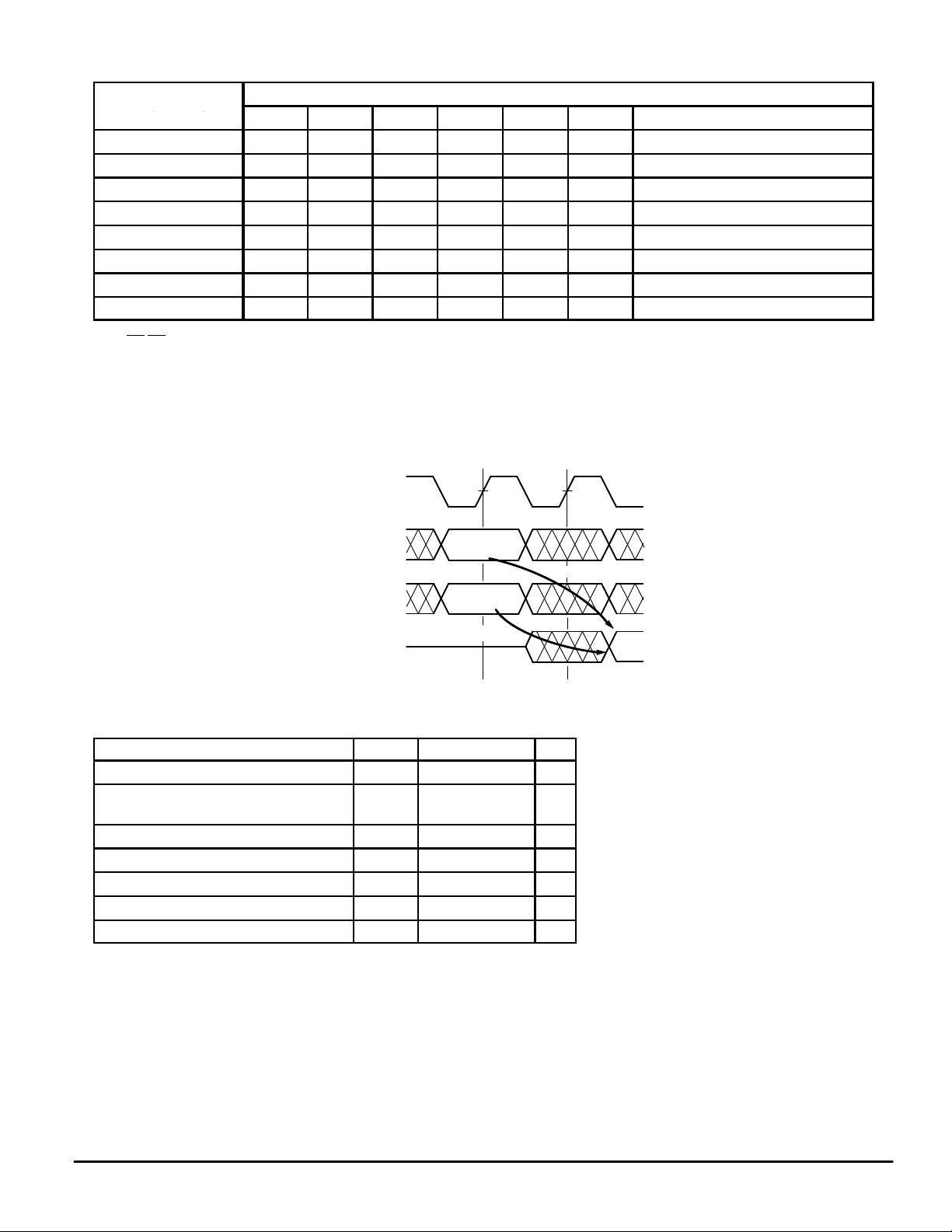
K
ADDRESS & CONTROL
DATA INPUT D
DATA OUTPUT Q
t
n
VALID
VALID
PASS–THROUGH
tn +
PIPELINED READ ACCESS
ABSOLUTE MAXIMUM RATINGS (See Note)
Rating
Power Supply Voltage V
Voltage Relative to VSS for Any Pin
Except V
Output Current I
Power Dissipation P
Temperature Under Bias T
Operating Temperature T
Storage Temperature — Plastic T
NOTE: Permanent device damage may occur if ABSOLUTE MAXIMUM RATINGS are
DD
exceeded. Functional operation should be restricted to RECOMMENDED OPERATING CONDITIONS. Exposure to higher than recommended voltages for extended
periods of time could affect device reliability.
Symbol Value Unit
DD
Vin, V
out
bias
stg
out
D
A
– 0.5 to + 4.6 V
– 0.5 to VDD + 0.5 V
± 20 mA
TBD W
– 10 to + 85 °C
0 to + 70 °C
– 55 to + 125 °C
1
VALID
This is a synchronous device. All synchronous inputs must meet specified setup and hold
times with stable logic levels for
edges of clock (K) while the device is selected.
This device contains circuitry to protect the
inputs against damage due to high static voltages or electric fields; however, it is advised
that normal precautions be taken to avoid
application of any voltage higher than maximum rated voltages to these high–impedance
circuits.
ALL
rising
MOTOROLA FAST SRAM
MCM69D618
5
 Loading...