

Motorola MCM64PE32SDG66, MCM64PE64SDG66 Datasheet
MOTOROLA
SEMICONDUCTOR TECHNICAL DATA
Advance Information
256K/512K Pipelined BurstRAM
Order this document
by MCM64PE32/D
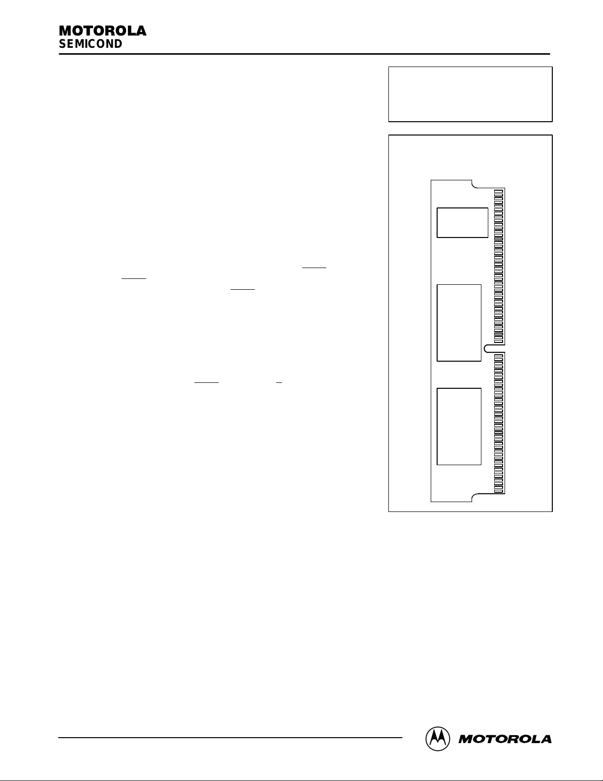
MCM64PE32
MCM64PE64
Secondary Cache Module
for Pentium
The MCM64PE32 (256K) and MCM64PE64 (512K) are designed to provide
a burstable, high performance, L2 cache for the Pentium microprocessor in
conjunction with Intel’s Triton II chip set. The MCM64PE32 is configured as 32K
x 64 bits and the MCM64PE64 is configured as 64K x 64 bits. Both are packaged
in a 160 pin card edge memory module. The MCM64PE32 module uses
Motorola’s 3.3 V 32K x 32 BurstRAMs and one Motorola 5 V 32K x 8 FSRAM for
the tag RAM. The MCM64PE64 module uses Motorola’s 3.3 V 64K x 32
BurstRAMs and one Motorola 5 V 32K x 8 FSRAM for the tag RAM.
Bursts can be initiated with either address status processor (ADSP
address status (CADS
the BurstRAM by the cache burst advance (CADV
Write cycles are internally self timed and are initiated by the rising edge of the
clock (CLK0) input. Eight write enables are provided for byte write control.
PD0 – PD3 map into the Triton II chip set for auto–configuration of the cache
control.
• Pentium–Style Burst Counter on Chip
• Pipelined Data Out
• 160 Pin Card Edge Module
• Address Pipeline Supported by ADSP
• All Cache Data and Tag I/Os are TTL Compatible
• Three State Outputs
• Byte Write Capability
• Fast Module Clock Rate: 66 MHz
• Fast SRAM Access Times:15 ns for Tag RAM
• One–Cycle Deselect Data RAMs
• Decoupling Capacitors for Each Fast Static RAM
• High Quality Multi–Layer FR4 PWB with Separate Power and Ground
Planes
• 8 Bits Tag RAM
• Dual Power Supplies: 3.3 V + 10%, – 5%
• Burndy Connector, Part Number: CELP2X80SC3Z48
• Intel COAST 3.0 Option III Compliant
• Burst Order Select (BOSEL) Option
). Subsequent burst addresses are generated internal to
) input pin.
Disabled with Ex
8 ns for Data RAMs
5 V ± 10%
) or cache
160–LEAD CARD EDGE
CASE TBD
TOP VIEW
1
42
43
80
BurstRAM is a trademark of Motorola.
Mfax is a trademark of Motorola.
Pentium is a trademark of Intel Corp.
This document contains information on a new product. Motorola reserves the right to change or discontinue this product without notice.
12/9/96
Motorola, Inc. 1996
MOTOROLA FAST SRAM
MCM64PE32•MCM64PE64
1
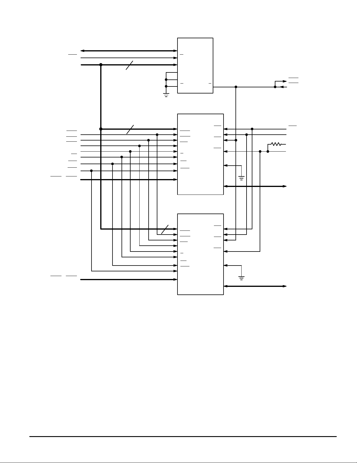
TIO0 – TIO7
TWE
A3 – A17
MCM64PE32 BLOCK DIAGRAM
32K x 8
DQ0 – DQ7
13
A5 – A17
W
A0 – A12
A13
A14
G
ECS2
E
ECS1
ADSP
CADS
CADV
CLK0
CG
BWE
GWE
CWE0 – CWE3
CWE4 – CWE7
15
15
32K x 32
SA0 – SA14
ADSP
ADSC
ADV
K
G
SW
SGW
SBa – SBd
DQ0 – DQ31
32K x 32
SA0 – SA14
ADSP
ADSC
ADV
K
G
SW
SGW
SBa – SBd
DQ0 – DQ31
SE1
SE2
SE3
LBO
ZZ
SE1
SE2
SE3
LBO
ZZ
4.7 k
CCS
V
DD
Ω
V
DD
BOSEL
DQ0 – DQ31
DQ32 – DQ63
MCM64PE32•MCM64PE64
2
MOTOROLA FAST SRAM
TIO0 – TIO7
TWE
A3 – A18
16
MCM64PE64 BLOCK DIAGRAM
32K x 32
DQ0 – DQ7
14
A5 – A18
W
A0 – A13
A14
G
E
ADSP
CADS
CADV
CLK0
CG
BWE
GWE
CWE0 – CWE3
CWE4 – CWE7
16
15
64K x 32
SA0 – SA15
ADSP
ADSC
ADV
K
G
SW
SGW
SBa – SBd
DQ0 – DQ31
64K x 32
SA0 – SA15
ADSP
ADSC
ADV
K
G
SW
SGW
SBa – SBd
DQ0 – DQ31
SE1
SE2
SE3
LBO
ZZ
SE1
SE2
SE3
LBO
ZZ
CCS
V
DD
DQ0 – DQ31
V
DD
4.7 k
Ω
BOSEL
DQ32 – DQ63
MOTOROLA FAST SRAM
MCM64PE32•MCM64PE64
3
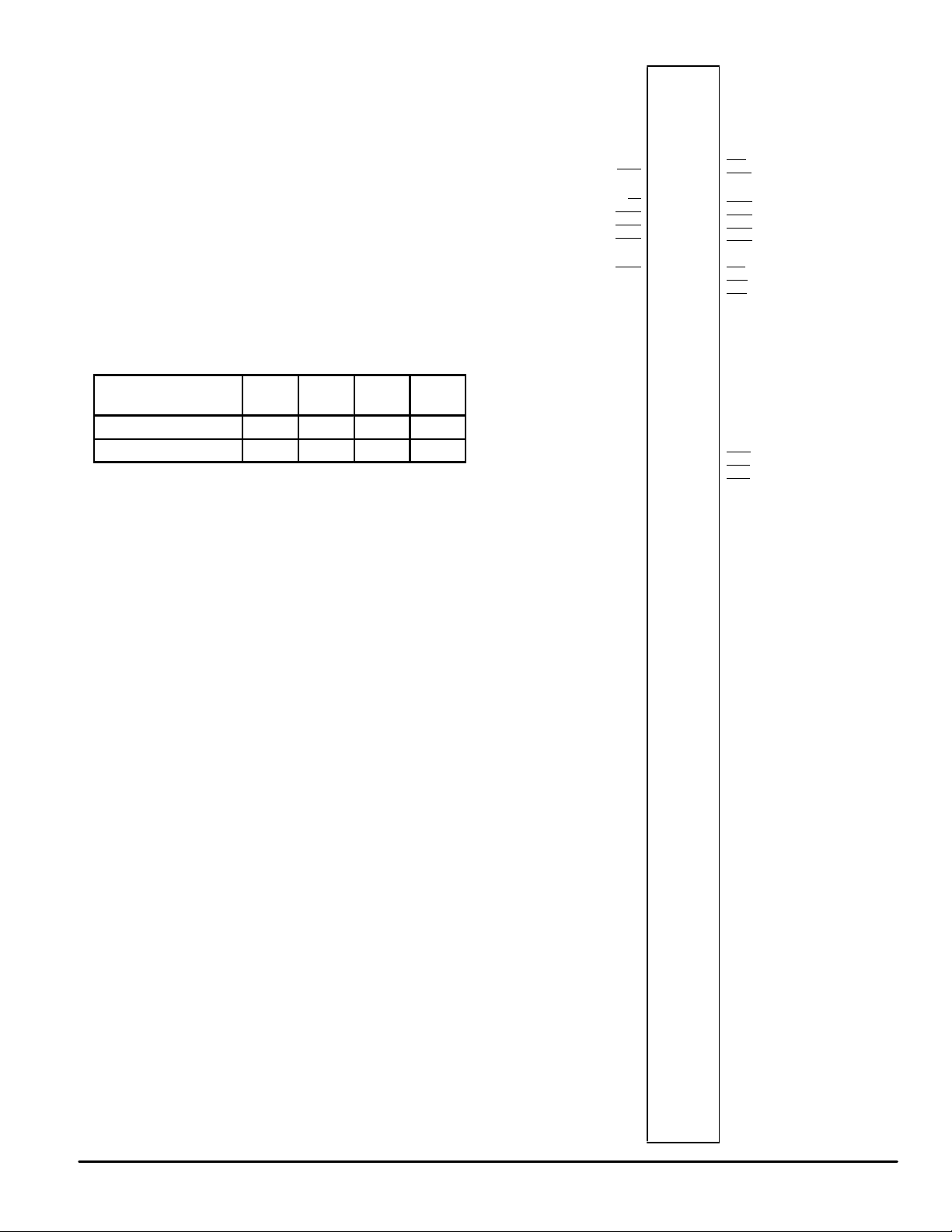
160–LEAD CARD EDGE MODULE
PRESENCE DETECT TABLE
Cache Size and
Functionality
256K Pipe Burst NC NC V
512K Pipe Burst NC NC NC V
PD0 PD1 PD2 PD3
PIN ASSIGNMENT
TOP VIEW
SS
NC
SS
V
SS
TIO1
TIO7
TIO5
TIO3
NC
VCC5
NC
CADV
V
SS
CG
CWE5
CWE7
CWE1
VCC5
CWE3
NC
NC
V
SS
RSVD
A4
A6
A8
A10
VCC5
A17
V
SS
A9
A14
A15
RSVD
PD0
PD2
BOSEL
V
SS
CLK0
V
SS
DQ63
VCC5
DQ61
DQ59
DQ57
81
82
83
84
85
86
87
88
89
90
91
92
93
94
95
96
97
98
99
100
101
102
103
104
105
106
107
108
109
110
111
112
113
114
115
116
117
118
119
120
121
122
V
1
SS
TIO0
2
TIO2
3
TIO6
4
TIO4
5
NC
6
VDD3
7
8
TWE
CADS
9
V
10
SS
11
CWE4
CWE6
12
CWE0
13
CWE2
14
VDD3
15
CCS
16
GWE
17
BWE
18
V
19
SS
A3
20
A7
21
A5
22
A11
23
A16
24
VDD3
25
A18
26
V
27
SS
A12
28
A13
29
ADSP
30
ECS1
31
ECS2
32
PD1
33
PD3
34
V
35
SS
NC
36
V
37
SS
DQ62
38
VDD3
39
DQ60
40
DQ58
41
DQ56
42
V
SS
DQ55
DQ53
DQ51
DQ49
V
SS
DQ47
DQ45
DQ43
VCC5
DQ41
DQ39
DQ37
V
SS
DQ35
DQ33
DQ31
VCC5
DQ29
DQ27
DQ25
V
SS
DQ23
DQ21
DQ19
VCC5
DQ17
DQ15
DQ13
V
SS
DQ11
DQ9
DQ7
VCC5
DQ5
DQ3
DQ1
V
SS
123
124
125
126
127
128
129
130
131
132
133
134
135
136
137
138
139
140
141
142
143
144
145
146
147
148
149
150
151
152
153
154
155
156
157
158
159
160
43
V
SS
44
DQ54
45
DQ52
46
DQ50
47
DQ48
48
V
SS
49
DQ46
50
DQ44
51
DQ42
52
VDD3
53
DQ40
54
DQ38
55
DQ36
56
V
SS
57
DQ34
58
DQ32
59
DQ30
60
V
DD
61
DQ28
62
DQ26
63
DQ24
64
V
SS
65
DQ22
66
DQ20
67
DQ18
68
VDD3
69
DQ16
70
DQ14
71
DQ12
72
V
SS
73
DQ10
74
DQ8
75
DQ6
76
VDD3
77
DQ4
78
DQ2
79
DQ0
80
V
SS
MCM64PE32•MCM64PE64
4
MOTOROLA FAST SRAM
PIN DESCRIPTIONS
160–Lead Card Edge Pin Locations Symbol
20, 21, 22, 23, 24, 26, 28, 29,
101, 102, 103, 104, 106, 108, 109, 110
30 ADSP Input Address Status Processor: Initiates READ, WRITE, or chip deselect
114 BOSEL Input Burst Order Select: NC for interleaved burst counter. Tie to ground for
18 BWE Input Byte Write Enable: To be used in future modules.
9 CADS Input Cache Address Status: Initiates READ, WRITE, or chip deselect cycle.
89 CADV Input Cache Burst Advance: Increments address count in accordance with
16 CCS Input Chip Select: Active low chip enable for data RAMs.
91 CG Input Cache Output Enable: Active low asynchronous input.
116 CLK0 Input Clock: This signal registers the address, data in, and all control signals
11, 12, 13, 14, 92, 93, 94, 96 CWE0 –
38, 40, 41, 42, 44, 45, 46, 47, 49, 50, 51,
53, 54, 55, 57, 58, 59, 61, 62, 63, 65, 66,
67, 69, 70, 71, 73, 74, 75, 77, 78, 79,
118, 120, 121, 122, 124, 125, 126, 127,
129, 130, 131, 133, 134, 135, 137, 138,
139, 141, 142, 143, 145, 146, 147, 149,
150, 151, 153, 154, 155, 157, 158, 159
31, 32 ECS1,
17 GWE Input Global Write Enable: To be used in future modules.
33, 34, 112, 113 PD0 –
100, 111 RSVD — No Connection: Reserved for future use.
2, 3, 4, 5, 82, 83, 84, 85 TIO0 –
8 TWE Input Tag Write Enable: Active low write signal for tag RAMs.
87, 95, 105, 119, 132, 140, 148, 156 VCC5 Supply Power Supply: 5.0 V ± 5%.
7, 15, 25, 39, 52, 60, 68, 76 VDD3 Supply Power Supply: 3.3 V + 10%, – 5%.
1, 10, 19, 27, 35, 37, 43, 48, 56, 64, 72,
80, 81, 90, 99, 107, 115, 117, 123, 128,
136, 144, 152, 160
6, 36, 86, 88, 97, 98 NC — No Connection: There is no connection to the module.
A3 – A18 Input Address Inputs: These inputs are registered into data RAMs and must
CWE7
DQ0 –
DQ63
ECS2
PD3
TIO7
V
SS
Type Description
meet setup and hold times. The tag RAM addresses are not registered.
cycle (Exception — chip deselect does not occur when ADSP
asserted and CCS
linear burst counter.
interleaved count style.
Low — enables output buffers (DQ pins)
High — DQx pins are high impedance.
except CG
Input Cache Data Byte Write Enable: Active low write signal for data RAMs.
I/O Synchronous Data I/O:
Drives data out of data RAMs during READ cycles.
Stores data to data RAMs during WRITE cycles.
Input Expansion Chip Select.
— Presence Detect: See Presence Detect Table.
I/O Tag RAM I/O:
Drives data out during tag compare cycles.
Stores data to tag RAM during tag WRITE cycles.
Supply Ground.
.
is high.
is
MOTOROLA FAST SRAM
MCM64PE32•MCM64PE64
5
 Loading...