

Motorola MCM63Z819TQ11, MCM63Z819TQ11R, MCM63Z819TQ15, MCM63Z819TQ15R, MCM63Z737TQ15 Datasheet
...
MOTOROLA
SEMICONDUCTOR TECHNICAL DATA
Advance Information
128K x 36 and 256K x 18 Bit
Flow–Through ZBT RAM
Synchronous Fast Static RAM
Order this document
by MCM63Z737/D
MCM63Z737
MCM63Z819
The ZBT RAM is a 4M–bit synchronous fast static RAM designed to provide
zero bus turnaround. The ZBT RAM allows 100% use of bus cycles during
back–to–back read/write and write/read cycles. The MCM63Z737 is organized
as 128K words of 36 bits each and the MCM63Z819 is organized as 256K words
of 18 bits each, fabricated with high performance silicon gate CMOS technology .
This device integrates input registers, a 2–bit address counter, and high speed
SRAM onto a single monolithic circuit for reduced parts count in communication
applications. Synchronous design allows precise cycle control with the use of an
external clock (CK). CMOS circuitry reduces the overall power consumption of
the integrated functions for greater reliability .
Addresses (SA), data inputs (DQ), and all control signals except output enable
) and linear burst order (LBO) are clock (CK) controlled through positive–
(G
edge–triggered noninverting registers.
Write cycles are internally self–timed and are initiated by the rising edge of the
clock (CK) input. This feature eliminates complex off–chip write pulse generation
and provides increased timing flexibility for incoming signals.
For read cycles, a flow–through SRAM allows output data to simply flow freely
from the memory array .
• 3.3 V L VTTL and LVCMOS Compatible
• MCM63Z737/MCM63Z819–11 = 11 ns Access/15 ns Cycle (66 MHz)
MCM63Z737/MCM63Z819–15 = 15 ns Access/20 ns Cycle (50 MHz)
• Selectable Burst Sequencing Order (Linear/Interleaved)
• Internally Self–Timed Write Cycle
• Single–Cycle Deselect
• Byte Write Control
• ADV Controlled Burst
• 100–Pin TQFP Package
TQ PACKAGE
TQFP
CASE 983A–01
ZBT and Zero Bus Turnaround are trademarks of Integrated Device Technology, Inc., and the architecture is supported by
Micron Technology, Inc. and Motorola, Inc.
This document contains information on a new product. Specifications and information herein are subject to change without notice.
2/6/98
Motorola, Inc. 1998
MOTOROLA FAST SRAM
MCM63Z737DMCM63Z819
1
PIN ASSIGNMENT
V
DDQ
V
DDQ
V
V
DQd
V
DDQ
DQd
DQd
DQd
DQd
V
DDQ
DQd
DQd
DQd
DQc
DQc
DQc
V
SS
DQc
DQc
DQc
DQc
V
SS
DQc
DQc
V
SS
DD
DD
V
SS
DQd
V
SS
V
SS
1
2
3
4
5
6
7
8
9
10
11
12
13
14
15
16
17
18
19
20
21
22
23
24
25
26
27
28
29
30
31 3233
SASASE1
DD
SE2
SBc
SBa
SBb
SBd
94 93979695 89889291 90 8685871009998 81828384
3738343536 42433940 41 454644
SE3
CK
VSSV
SW
CKE
G
ADV
NC
NC
SA
50494847
80
79
78
77
76
75
74
73
72
71
70
69
68
67
66
65
64
63
62
61
60
59
58
57
56
55
54
53
52
51
SA
DQb
DQb
DQb
V
DDQ
V
SS
DQb
DQb
DQb
DQb
V
SS
V
DDQ
DQb
DQb
V
SS
V
SS
V
DD
V
SS
DQa
DQa
V
DDQ
V
SS
DQa
DQa
DQa
DQa
V
SS
V
DDQ
DQa
DQa
DQa
SASASA
LBO
SA
NC
SA1
SA0
TOP VIEW
MCM63Z737
NC
V
SS
DD
V
NC
NC
SASASA
SA
SA
SA
SA
MCM63Z737DMCM63Z819
2
MOTOROLA FAST SRAM
PIN ASSIGNMENT
V
DDQ
DQb
DQb
V
DDQ
DQb
DQb
V
V
DQb
DQb
V
DDQ
DQb
DQb
DQb
V
DDQ
V
V
V
V
V
V
NC
NC
NC
SS
NC
NC
SS
SS
DD
DD
SS
SS
NC
SS
NC
NC
NC
1
2
3
4
5
6
7
8
9
10
11
12
13
14
15
16
17
18
19
20
21
22
23
24
25
26
27
28
29
30
31 3233
SASASE1
DD
SE2
NC
SBa
SBb
NC
94 93979695 89889291 90 8685871009998 81828384
3738343536 42433940 41 454644
SE3
CK
VSSV
SW
CKE
G
ADV
NC
NC
SA
50494847
80
79
78
77
76
75
74
73
72
71
70
69
68
67
66
65
64
63
62
61
60
59
58
57
56
55
54
53
52
51
SA
SA
NC
NC
V
DDQ
V
SS
NC
DQa
DQa
DQa
V
SS
V
DDQ
DQa
DQa
V
SS
V
SS
V
DD
V
SS
DQa
DQa
V
DDQ
V
SS
DQa
DQa
NC
NC
V
SS
V
DDQ
NC
NC
NC
SASASA
LBO
SA
NC
SA1
SA0
TOP VIEW
MCM63Z819
NC
V
SS
DD
V
NC
NC
SASASA
SA
SA
SA
SA
MOTOROLA FAST SRAM
MCM63Z737DMCM63Z819
3
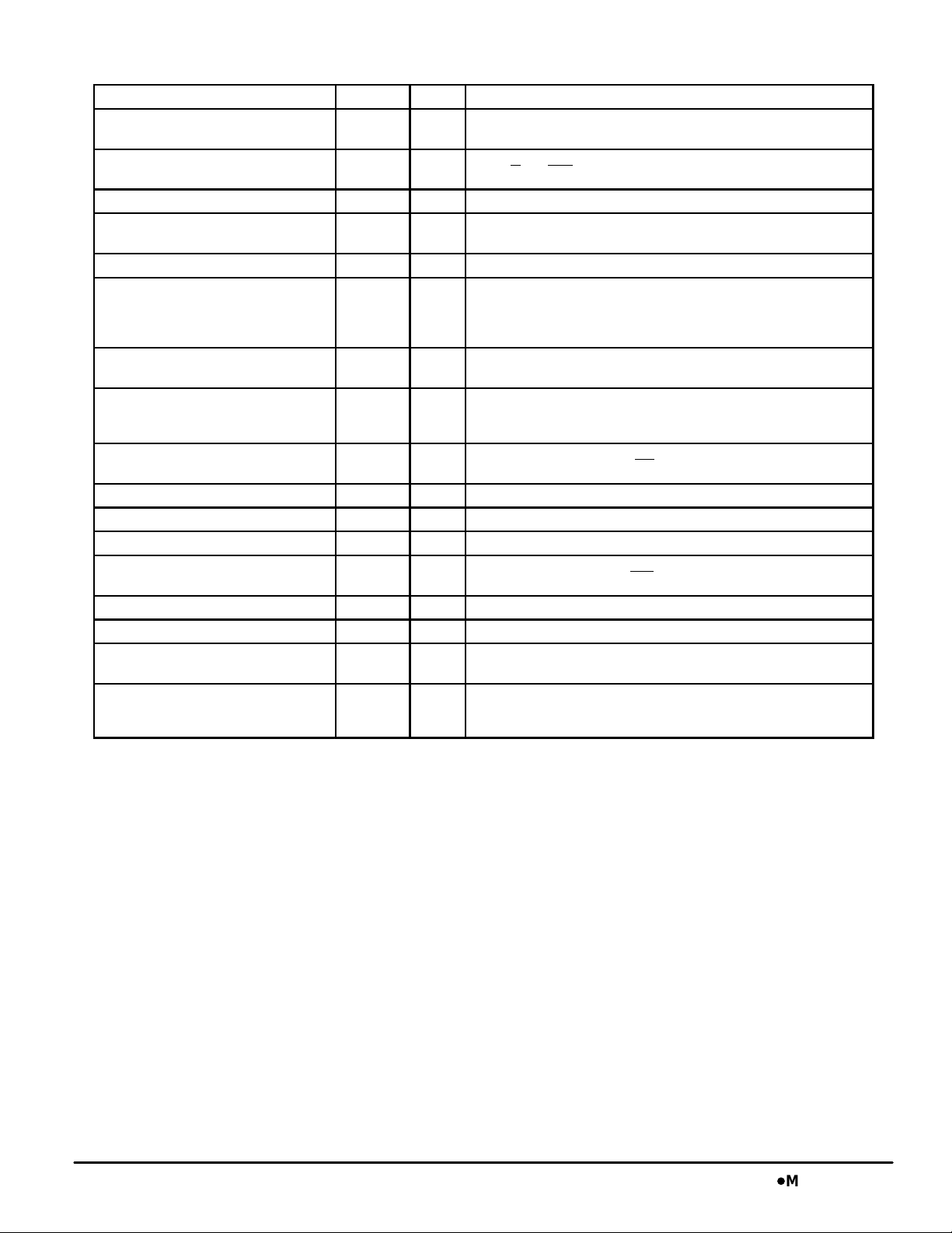
MCM63Z737 PIN DESCRIPTIONS
Pin Locations Symbol
85 ADV Input Synchronous Load/Advance: Loads a new address into counter when
89 CK Input Clock: This signal registers the address, data in, and all control signals
87 CKE Input Clock Enable: Disables the CK input when CKE is high.
(a) 51, 52, 53, 56, 57, 58, 59, 62, 63
(b) 68, 69, 72, 73, 74, 75, 78, 79, 80
(c) 1, 2, 3, 6, 7, 8, 9, 12, 13
(d) 18, 19, 22, 23, 24, 25, 28, 29, 30
86 G Input Asynchronous Output Enable.
31 LBO Input Linear Burst Order Input: This pin must remain in steady state (this
32, 33, 34, 35, 44, 45, 46,
47, 48, 49, 50, 81, 82, 99, 100
36, 37 SA0, SA1 Input Synchronous Burst Address Inputs: The two LSB’s of the address field.
93, 94, 95, 96
(a) (b) (c) (d)
98 SE1 Input Synchronous Chip Enable: Active low to enable chip.
97 SE2 Input Synchronous Chip Enable: Active high for depth expansion.
92 SE3 Input Synchronous Chip Enable: Active low for depth expansion.
88 SW Input Synchronous Write: This signal writes only those bytes that have been
15, 16, 41, 65, 91 V
4, 11, 20, 27, 54, 61, 70, 77 V
5, 10, 14, 17, 21, 26, 40,
55, 60, 64, 66, 67, 71, 76, 90
38, 39, 42, 43, 83, 84 NC — No Connection: There is no connection to the chip.
Type Description
low. RAM uses internally generated burst addresses when high.
except G
DQx I/O Synchronous Data I/O: “x” refers to the byte being read or written
SA Input Synchronous Address Inputs: These inputs are registered and must
SBx Input Synchronous Byte Write Inputs: Enables write to byte “x”
DD
DDQ
V
SS
Supply Core Power Supply.
Supply I/O Power Supply.
Supply Ground.
(byte a, b, c, d).
signal not registered or latched). It must be tied high or low.
Low – linear burst counter.
High – interleaved burst counter.
meet setup and hold times.
These pins must preset the burst address counter values. These inputs
are registered and must meet setup and hold times.
(byte a, b, c, d) in conjunction with SW
selected using the byte write SBx
and LBO.
. Has no effect on read cycles.
pins.
MCM63Z737DMCM63Z819
4
MOTOROLA FAST SRAM
MCM63Z819 PIN DESCRIPTIONS
Pin Locations Symbol Type Description
85 ADV Input Synchronous Load/Advance: Loads a new address into counter when
89 CK Input Clock: This signal registers the address, data in, and all control signals
87 CKE Input Clock Enable: Disables the CK input when CKE is high.
(a) 58, 59, 62, 63, 68, 69, 72, 73, 74
(b) 8, 9, 12, 13, 18, 19, 22, 23, 24
86 G Input Asynchronous Output Enable.
31 LBO Input Linear Burst Order Input: This pin must remain in steady state (this
32, 33, 34, 35, 44, 45, 46,
47, 48, 49, 50, 80, 81, 82, 99, 100
36, 37 SA0, SA1 Input Synchronous Burst Address Inputs: The two LSB’s of the address field.
93, 94
(a) (b)
98 SE1 Input Synchronous Chip Enable: Active low to enable chip.
97 SE2 Input Synchronous Chip Enable: Active high for depth expansion.
92 SE3 Input Synchronous Chip Enable: Active low for depth expansion.
88 SW Input Synchronous Write: This signal writes only those bytes that have been
15, 16, 41, 65, 91 V
4, 11, 20, 27, 54, 61, 70, 77 V
5, 10, 14, 17, 21, 26, 40,
55, 60, 64, 66, 67, 71, 76, 90
1, 2, 3, 6, 7, 25, 28, 29, 30, 38,
39, 42, 43, 51, 52, 53, 56, 57,
75, 78, 79, 83, 84, 95, 96
low. RAM uses internally generated burst addresses when high.
except G
DQx I/O Synchronous Data I/O: “x” refers to the byte being read or written
SA Input Synchronous Address Inputs: These inputs are registered and must
SBx Input Synchronous Byte Write Inputs: Enables write to byte “x”
DD
DDQ
V
SS
NC — No Connection: There is no connection to the chip.
Supply Core Power Supply.
Supply I/O Power Supply.
Supply Ground.
(byte a, b).
signal not registered or latched). It must be tied high or low.
Low – linear burst counter.
High – interleaved burst counter.
meet setup and hold times.
These pins must preset the burst address counter values. These inputs
are registered and must meet setup and hold times.
(byte a, b) in conjunction with SW
selected using the byte write SBx
and LBO.
. Has no effect on read cycles.
pins.
MOTOROLA FAST SRAM
MCM63Z737DMCM63Z819
5
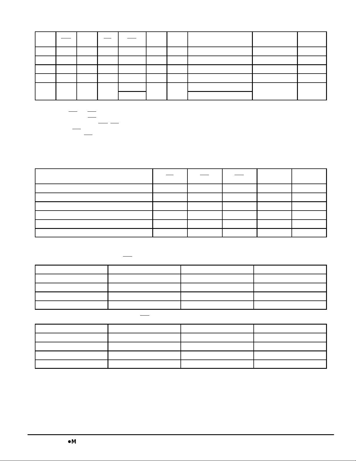
TRUTH TABLE
SA0 –
CK CKE E SW SBx ADV
L–H 1 X X X X X Hold H 1, 2
L–H 0 False X X 0 X Deselect D 1, 2
L–H 0 True 0 V 0 V Load Address, New Write W 1, 2, 3, 4, 5
L–H 0 True 1 X 0 V Load Address, New Read R 1, 2
L–H 0 X X
NOTES:
1. X = don‘t care, 1 = logic high, 0 = logic low, V = valid signal, according to AC Operating Conditions and Characteristics.
2. E = true if SE1
3. Byte write enables, SBx
4. No control inputs except CKE
5. A write with SBx
6. A burst write with SBx
7. ADV controls whether the RAM enters burst mode. If the previous cycle was a write, then ADV = 1 results in a burst write. If the previous
cycle is a read, then ADV = 1 results in a burst read. ADV = 1 will also continue a deselect cycle.
and SE3 = 0, and SE2 = 1.
, are evaluated only as new write addresses are loaded.
, SBx, and ADV are recognized in a clock cycle where ADV is sampled high.
not valid does load addresses.
not valid does increment address.
V (W)
X (R, D) Continue
1 X
SAx
Next Operation
Burst
Input Command
Code
B 1, 2, 4,
Notes
WRITE TRUTH TABLE
SBc
Cycle Type SW SBa SBb
Read H X X X X
Write Byte a L L H H H
Write Byte b L H L H H
Write Byte c (See Note 1) L H H L H
Write Byte d (See Note 1) L H H H L
Write All Bytes L L L L L
NOTE:
1. Valid only for MCM63Z737.
(See Note 1)
SBd
(See Note 1)
6, 7
LINEAR BURST ADDRESS TABLE (LBO = V
1st Address (External) 2nd Address (Internal) 3rd Address (Internal) 4th Address (Internal)
X . . . X00 X . . . X01 X . . . X10 X . . . X11
X . . . X01 X . . . X10 X . . . X11 X . . . X00
X . . . X10 X . . . X11 X . . . X00 X . . . X01
X . . . X11 X . . . X00 X . . . X01 X . . . X10
INTERLEAVED BURST ADDRESS TABLE (LBO = V
1st Address (External) 2nd Address (Internal) 3rd Address (Internal) 4th Address (Internal)
X . . . X00 X . . . X01 X . . . X10 X . . . X11
X . . . X01 X . . . X00 X . . . X11 X . . . X10
X . . . X10 X . . . X11 X . . . X00 X . . . X01
X . . . X11 X . . . X10 X . . . X01 X . . . X00
SS
)
)
DD
MCM63Z737DMCM63Z819
6
MOTOROLA FAST SRAM
 Loading...