

Motorola MCM56824AZP35R2, MCM56824AZP25R2, MCM56824AZP20, MCM56824AZP20R2, MCM56824AZP25 Datasheet
...
MCM56824A
1
MOTOROLA FAST SRAM
DSPRAM
8K x 24 Bit Fast Static RAM
The MCM56824A is a 196,608 bit static random access memory organized as
8,192 words of 24 bits. The device integrates an 8K x 24 SRAM core with multiple
chip enable inputs, output enable, and an externally controlled single address pin
multiplexer. These functions allow for direct connection to the Motorola
DSP56001 Digital Signal Processor and provide a very efficient means for implementation of a reduced parts count system requiring no additional interface logic.
The availability of multiple chip enable (E1
and E2) and output enable (G) inputs provides for greater system flexibility when multiple devices are used. With
either chip enable input unasserted, the device will enter standby mode, useful
in low–power applications. A single on–chip multiplexer selects A12 or X/Y
as the
highest order address input depending upon the state of the V/S
control input.
This feature allows one physical static RAM component to efficiently store program and vector or scalar operands by dynamically re–partitioning the RAM
array. T ypical applications will logically map vector operands into upper memory
with scalar operands being stored in lower memory. By connecting
DSP56001address A15 to the VECTOR/SCALAR (V/S
) MUX control
pin, such partitioning can occur with no additional components. This allows efficient utilization of the RAM resource irrespective of operand
type. See application diagrams at the end of this document for additional information.
Multiple power and ground pins have been utilized to minimize effects
induced by output noise.
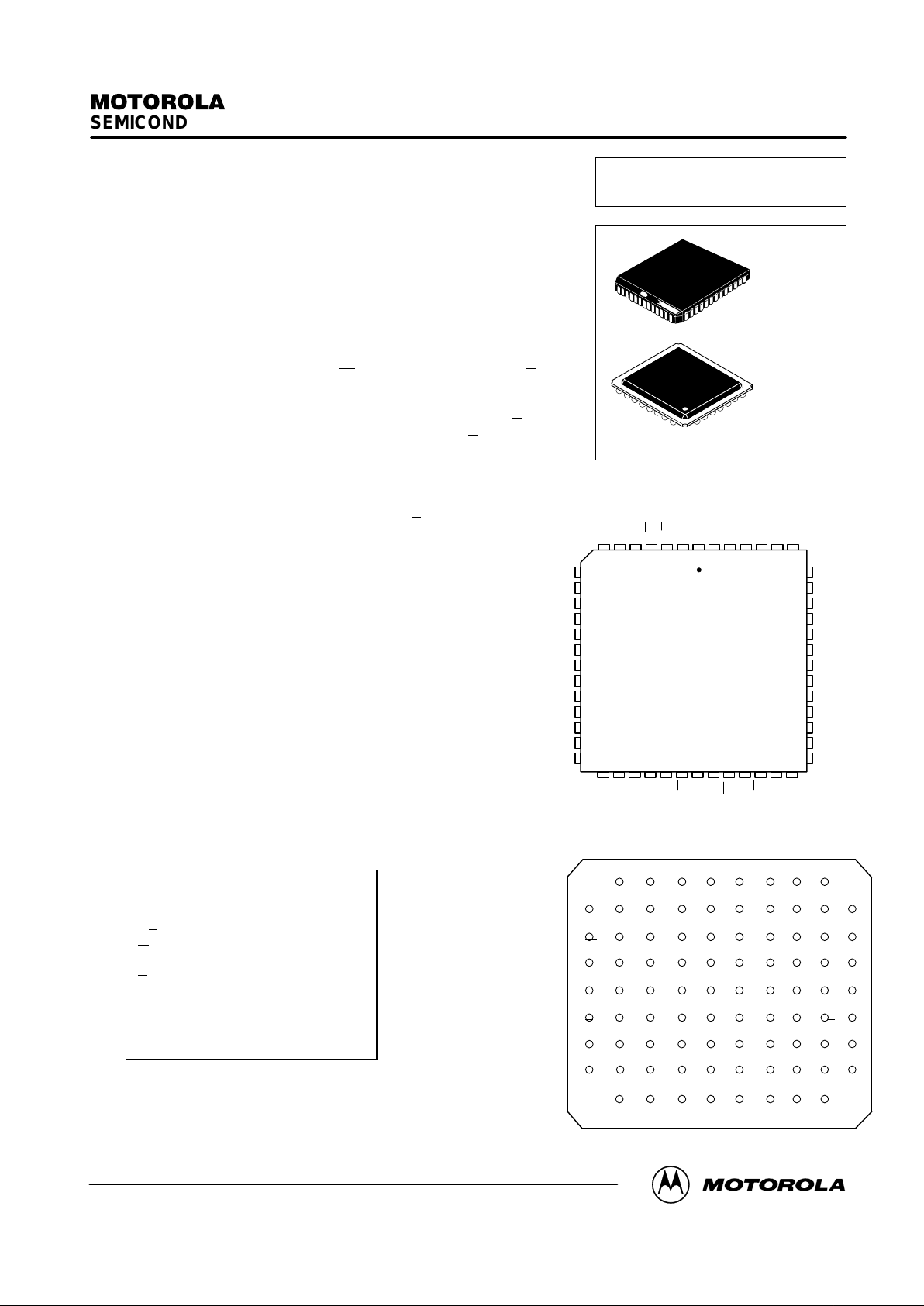
The MCM56824A is available in a 52 pin plastic leaded chip–carrier
(PLCC) and a 9 x 10 grid, 86 bump surface mount PBGA.
• Single 5 V ± 10% Power Supply
• Fast Access and Cycle Times: 20/25/35 ns Max
• Fully Static Read and Write Operations
• Equal Address and Chip Enable Access Times
• Single Bit On–Chip Address Multiplexer
• Active High and Active Low Chip Enable Inputs
• Output Enable Controlled Three State Outputs
• High Board Density PLCC Package
• Low Power Standby Mode
• Fully TTL Compatible
DSPRAM is a trademark of Motorola, Inc.
For proper operation of the device, all V
SS
pins must be connected to ground.
PIN NAMES
A0 – A11 Address Inputs. . . . . . . . . . . . . . .
A12, X/Y
Multiplexed Address. . . . . . . . . .
V/S
Address Multiplexer Control. . . . . . . . .
W
Write Enable. . . . . . . . . . . . . . . . . . . . . . .
E1
, E2 Chip Enable. . . . . . . . . . . . . . . . . . .
G
Output Enable. . . . . . . . . . . . . . . . . . . . . .
DQ0 – DQ23 Data Input/Output. . . . . . . . . .
V
CC
+5 V Power Supply. . . . . . . . . . . . . . .
V
SS
Ground. . . . . . . . . . . . . . . . . . . . . . . . . .
NC No Connection. . . . . . . . . . . . . . . . . . . .
PIN ASSIGNMENTS
DQ0
DQ1
DQ2
V
SS
DQ3
DQ4
DQ5
DQ6
DQ7
DQ8
V
SS
DQ9
DQ10
DQ23
DQ22
DQ21
V
SS
DQ20
DQ19
DQ18
DQ17
DQ16
DQ15
V
SS
DQ14
DQ13
DQ11
A9A8A7
A6
DQ12
NC
W
G
CC
SS
E1
E2
V
V
8
9
10
11
12
13
14
15
16
17
18
19
20
46
45
44
43
42
41
40
39
38
37
36
35
34
4748495051521234567
33323130292827262524232221
A10
A11
A12
A5
A4
A3
A2
A1
A0
CC
V
NC
X/Y
V/S
PLCC
D21
V
SS
V
SS
A0
V
CC
NC
X/Y
A11
A2
A4
A3
D23
A1
V/S
A12
A10
D0
D22
D20D17D16
D15D14
D13
D12
D1
D2
V
SS
D5
D8
D7V
SS
D9D11
D10
E2
A6
A8
W
E1
V
CC
G
A7
A9
V
SS
A5
D18
D19
V
SS
D3
D4
D6
98765410
B
C
G
A
D
E
F
H
J
Not to Scale
321
VIEW OF PBGA PACKAGE BOTTOM
Order this document
by MCM56824A/D
MOTOROLA
SEMICONDUCTOR TECHNICAL DATA
MCM56824A
FN PACKAGE
52–LEAD PLCC
CASE 778–02
9 x 10 GRID
86 BUMP PBGA
CASE 896A–01
REV 2
4/95
Motorola, Inc. 1995
MCM56824A
2
MOTOROLA FAST SRAM
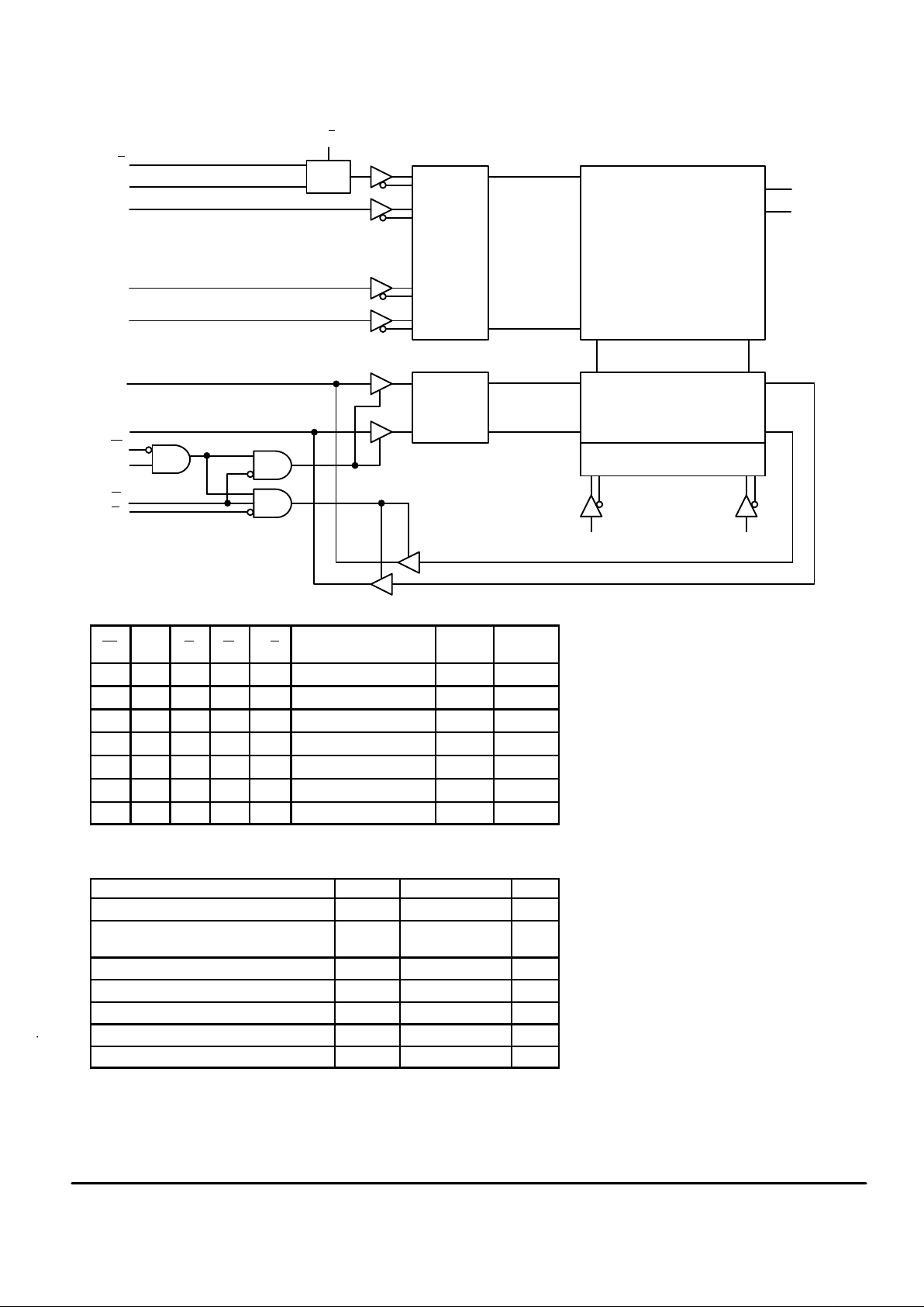
BLOCK DIAGRAM
Q
0
1
INPUT
DATA
CONTROL
(MSB)
(LSB)
V/S
A9
A6
DQ23
MEMORY ARRA Y
512 ROWS x
384 COLUMNS
ROW
DECODER
COLUMN DECODER
COLUMN I/O
V
CC
A11
A10
A5
A0
A12
X/Y
G
W
E1
E2
DQ0
A12
2 TO 1 MUX
•
•
•
•••
•••
•
•
•
•
•
•
•
•
•
•
•
•
V
SS
TRUTH TABLE
E1 E2 G W V/S Mode
Supply
Current
I/O
Status
H X X X X Not Selected I
SB
High–Z
X L X X X Not Selected I
SB
High–Z
L H H H X Output Disable I
CC
High–Z
L H L H H Read Using X/Y I
CC
Data Out
L H L H L Read Using A12 I
CC
Data Out
L H X L H Write Using X/Y I
CC
Data In
L H X L L Write Using A12 I
CC
Data In
NOTE: X=don’t care.
ABSOLUTE MAXIMUM RATINGS (Voltages Referenced to V
SS
= 0 V)
Rating
Symbol Value Unit
Power Supply Voltage V
CC
– 0.5 to + 7.0 V
Voltage Relative to VSS for Any Pin
Except V
CC
Vin, V
out
– 0.5 to VCC + 0.5 V
Output Current (per I/O) I
out
± 20 mA
Power Dissipation P
D
1.75 W
Temperature Under Bias T
bias
– 10 to + 85 °C
Operating Temperature T
A
0 to + 70 °C
Storage Temperature T
stg
– 55 to + 125 °C
NOTE: Permanent device damage may occur if ABSOLUTE MAXIMUM RATINGS are
exceeded. Functional operation should be restricted to RECOMMENDED OPERATING CONDITIONS. Exposure to higher than recommended voltages for
extended periods of time could affect device reliability.
This device contains circuitry to protect
against damage due to high static voltages
or electric fields; however, it is advised that
normal precautions be taken to avoid application of any voltage higher than maximum
rated voltages to this high–impedance
circuit.
This CMOS memory circuit has been designed to meet the dc and ac specifications
shown in the tables, after thermal equilibrium has been established. The circuit is
assumed to be in a test socket or mounted
on a printed circuit board with at least 300
LFPM of transverse air flow being
maintained.
MCM56824A
3
MOTOROLA FAST SRAM
DC OPERA TING CONDITIONS AND CHARACTERISTICS
(VCC = 5.0 V ± 10%, TA = 0 to + 70°C, Unless Otherwise Noted)
RECOMMENDED OPERATING CONDITIONS
(Voltages Referenced to VSS = 0 V)
Parameter
Symbol Min Typ Max Unit
Supply Voltage (Operating Voltage Range) V
CC
4.5 5.0 5.5 V
Input High Voltage V
IH
2.2 —
VCC + 0.3
V
Input Low Voltage V
IL
– 0.5* — 0.8 V
*VIL (min) = – 3.0 V ac (pulse width ≤ 20 ns)
DC CHARACTERISTICS
Parameter Symbol Min Max Unit
Input Leakage Current (All Inputs, Vin = 0 to VCC) I
lkg(i)
— ± 1.0 µA
Output Leakage Current (G = VIH, E1 = VIH, E2 = VIL, V
out
= 0 to VCC) I
lkg(O)
— ± 1.0 µA
AC Supply Current (G = VIH, E1 = VIL, E2 = VIH, I
out
= 0 mA,
All Other Inputs ≥ VIL = 0.0 V and VIH ≥ 3.0 V) MCM56824A–20 Cycle Time: ≥20 ns
MCM56824A–25 Cycle Time: ≥ 25 ns
MCM56824A–35 Cycle Time: ≥ 35 ns
I
CCA
—
—
—
260
220
180
mA
Standby Current (E1 = VIH, E2 = VIL, All Inputs = VIL or VIH) I
SB1
— 15 mA
CMOS Standby Current (E1 ≥ VCC – 0.2 V, E2 ≤ 0.2 V , All Inputs ≥VCC – 0.2 V or ≤ 0.2 V) I
SB2
— 10 mA
Output Low Voltage (IOL = + 8.0 mA) V
OL
— 0.4 V
Output High Voltage (IOH = – 4.0 mA) V
OH
2.4 — V
CAPACITANCE (f = 1.0 MHz, dV = 3.0 V, T
A
= 25°C, Periodically Sampled Rather Than 100% Tested)
Parameter
Symbol Typ Max Unit
Input Capacitance All Pins Except DQ0 – DQ23 C
in
4 6 pF
Input/Output Capacitance DQ0 – DQ23 C
out
6 8 pF
OUTPUT
Z0 = 50
Ω
RL = 50
Ω
VL = 1.5 V
(a) (b)
5 pF
+ 5 V
OUTPUT
255
Ω
480
Ω
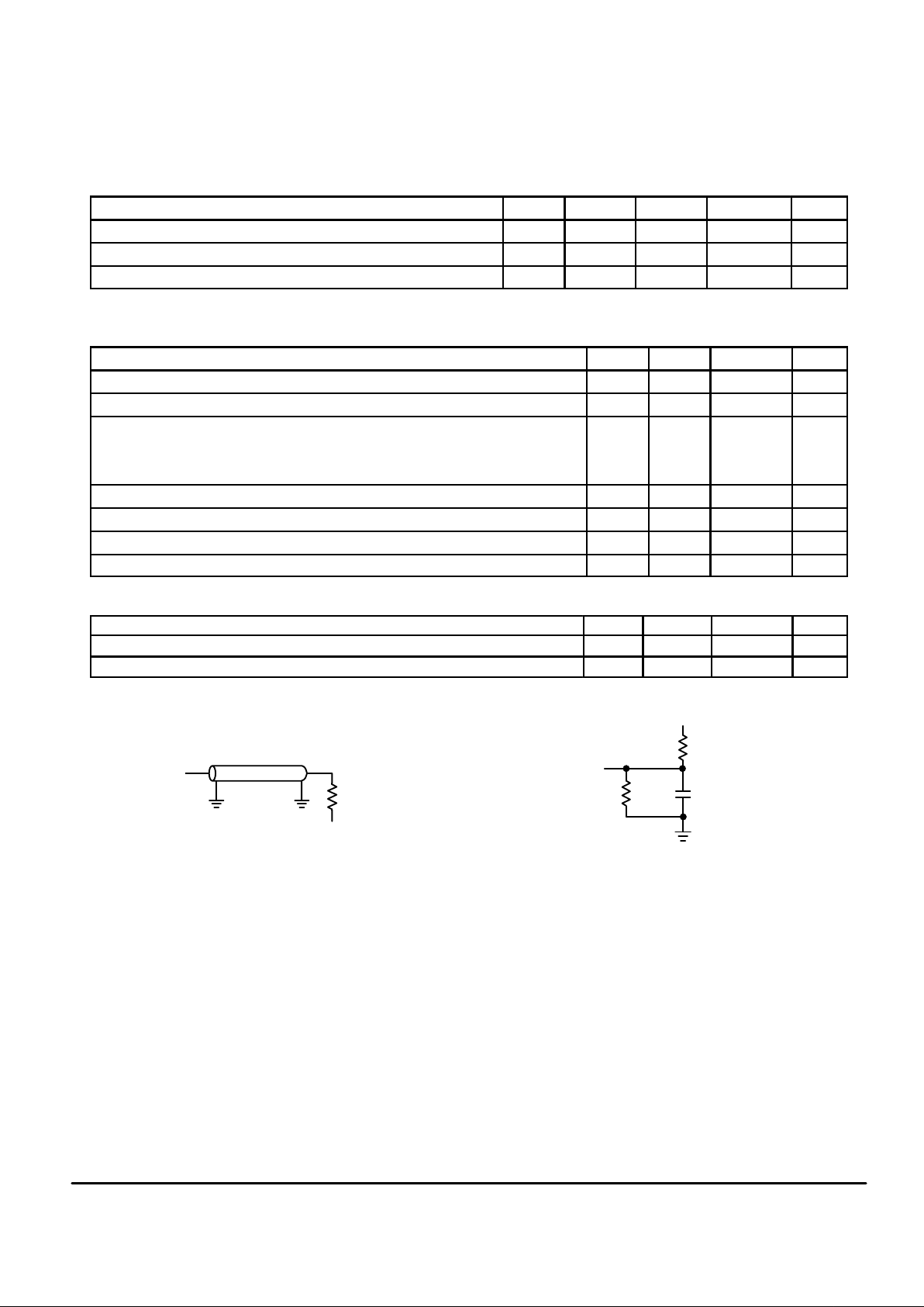
Figure 1. AC Test Loads
 Loading...