

MOTOROLA MCM4464 Technical data
MCM4464 SERIES
1
MOTOROLA FAST SRAM
1MB R4000 Secondary Cache
Fast Static RAM Module Set
Four MCM4464 modules comprise a full 1 MB of secondary cache for the
R4000 processor. Each module contains nine MCM6709J fast static RAMs for
a cache data size of 64K x 36. The tag portion, dependent on word line size,
contains either two MCM6709J or one MCM6706J fast static RAMs. All input signals, except A0 and WE
are buffered using 74FBT2827 drivers with series 25 Ω
resistors.
The MCM6709J and MCM6706J are fabricated using high–performance silicon–gate BiCMOS technology. Static design eliminates the need for internal
clocks or timing strobes.
All 1MB R4000 supported secondary cache options are available.
• Single 5 V ± 10% Power Supply
• All Inputs and Outputs are TTL Compatible
• Three State Outputs
• Fast Module Access Time: 12/15/17 ns
• Zero Wait–State Operation
• Unified or Split Seconday Cache Modules are Available (See Ordering
Information for Details)
• Word Line Sizes of 4, 8, 16, and 32 are Available (See Ordering
Information for Details)
• The Pin Compatible MCM44256 Series is also Available to Support a Full
4MB R4000 Secondary Cache.
• Decoupling Capacitors are Used for Each Fast Static RAM and Buffer,
Along with Bulk Capacitance for Maximum Noise Immunity
• High Quality Multi–Layer FR4 PWB with Separate Power and Ground
Planes
Write Enable. . . . . . . . . . . . . . . . . . . . . . .
DCS
Data Enable. . . . . . . . . . . . . . . . . . . . . .
TCS
Tag Enable. . . . . . . . . . . . . . . . . . . . . . .
OE
Output Enable. . . . . . . . . . . . . . . . . . . . .
DQ0 – DQ35 Data Input / Output. . . . . . . . .
TDQ0 – TDQ7 TAG Data Input / Output. . .
V
CC
+ 5 V Power Supply. . . . . . . . . . . . . . . .
V
SS
Ground. . . . . . . . . . . . . . . . . . . . . . . . . .
For proper operation of the device, VSS must
be connected to ground.
Order this document
by MCM4464/D
MOTOROLA
SEMICONDUCTOR TECHNICAL DATA
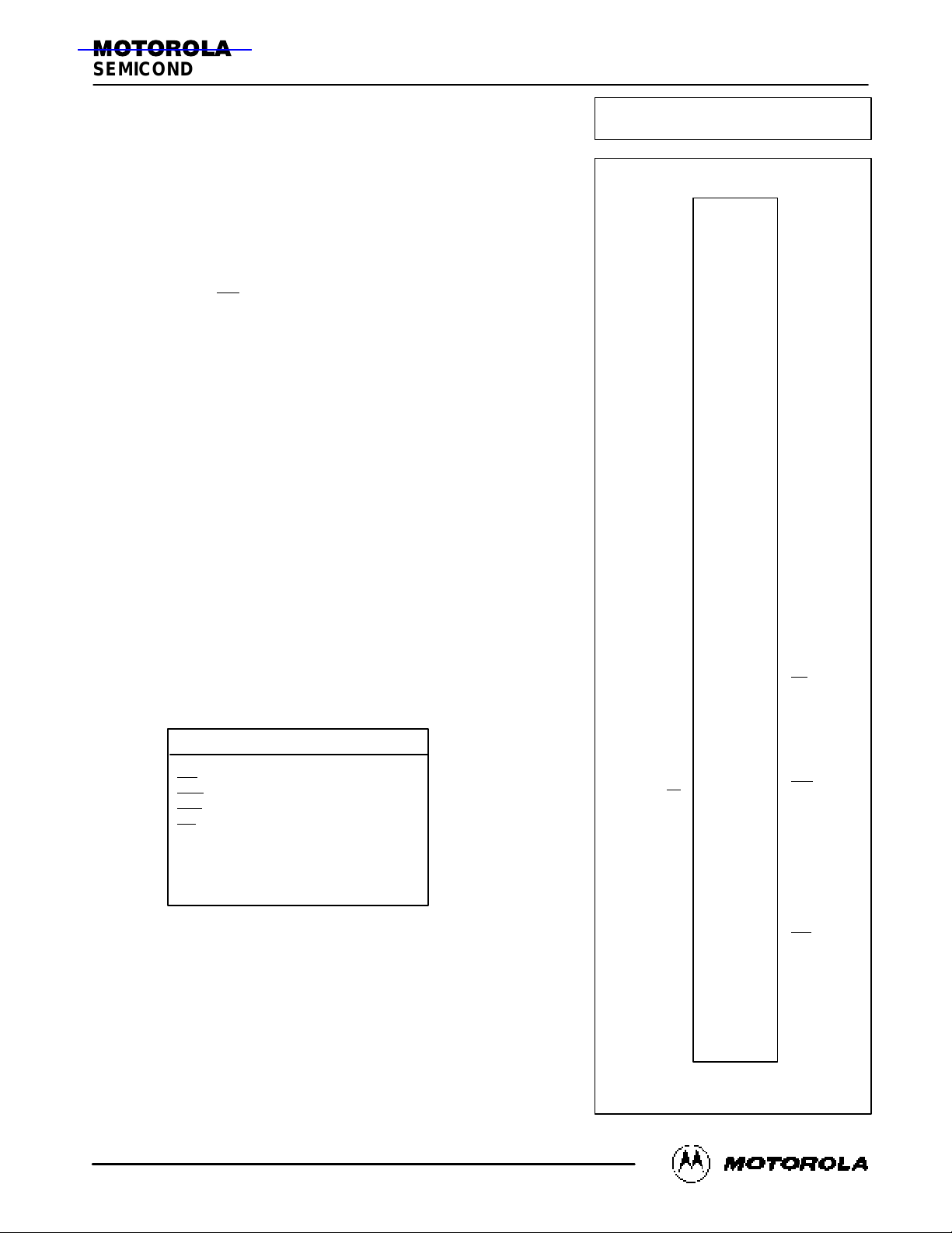
PIN ASSIGNMENT
80 LEAD SIMM — TOP VIEW
MCM4464 Series
VCC2
DQ5
V
SS
DQ8
DQ10
DQ12
DQ14
DQ15
DQ17
DQ19
DQ21
V
SS
DQ23
DQ25
DQ27
V
SS
DQ0
DQ2
DQ4
DQ6
DQ9
DQ11
DQ13
V
SS
DQ16
DQ18
DQ20
DQ22
V
CC
DQ28
DQ7
19
21
23
25
27
29
1
3
5
7
9
11
13
15
17
20
22
24
26
28
30
32
4
6
8
10
12
14
16
18
31
DQ3
33
35
37
34
36
38
40
39
DQ31
V
SS
DQ26
DQ24
DQ34 42
A0
A2
A4
A6
V
CC
OE
A8
A10
V
SS
A13
A15
NC
TDQ0
TDQ1
DQ33
DQ35
WE
A1
A3
V
SS
DCS
A7
A9
A11
A12
A14
NC
TCS
TDQ4
A5
59
61
63
65
67
69
41
43
45
47
49
51
53
55
57
60
62
64
66*
68*
70
72
44
46
48
50
52
54
56
58
71
V
SS
73
75
77
74
76
78
80
79 V
CC
TDQ6
TDQ2
V
SS
DQ29
DQ30
DQ32
DQ1
TDQ3
TDQ5
TDQ7
V
SS
NOTE: Pin assignment is for unified cache. For
split cache option, Pin 68 becomes
Address MSB (A15) and Pin 66 is NC.
REV 1
8/94
Motorola, Inc. 1994
查询MCM4464供应商
A0 – A15 Address Inputs. . . . . . . . . . . . . . . .
WE
PIN NAMES
MCM4464 SERIES
2
MOTOROLA FAST SRAM
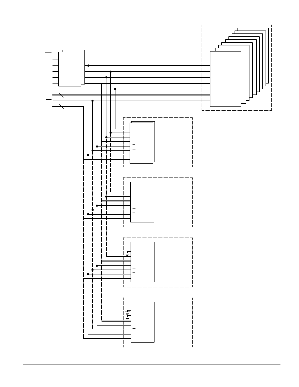
BLOCK DIAGRAM
A0
DQ0 – DQ3
W
MCM6709J
E
G
A1
A2
A3 – A15
A3 – A15
A0
DQ0 – DQ35
TCS
DCS
OE
A1
A2
WE
TDQ0 – TDQ7
74FBT2827
DRIVER
4 WORD
LINE SIZE
64K x 36 CACHE
TAG OPTIONS:
36
8
MCM6709J
MCM6706J
MCM6706J
MCM6706J
W
G
DQ0 – DQ7
A0
A1
A2 – A14
E
64K x 8
TAG
8 WORD
LINE SIZE
32K x 8
TAG
(A0 NOT USED)
16 WORD
LINE SIZE
16K x 8
TAG
(A0, A1 NOT USED)
32 WORD
LINE SIZE
8K x 8
TAG
(A0, A1, A2 NOT USED)
W
G
DQ0 – DQ7
A0
A1
A2 – A14
E
W
G
DQ0 – DQ7
A0
A1
A2 – A14
E
W
G
DQ0 – DQ7
A0
A1
A3 – A15
E
A2
MCM4464 SERIES
3
MOTOROLA FAST SRAM
ABSOLUTE MAXIMUM RATINGS (Voltages Referenced to V
SS
= 0 V)
Rating
Symbol Value Unit
Power Supply Voltage V
CC
– 0.5 to 7.0 V
Voltage Relative to V
SS
Vin, V
out
– 0.5 to VCC + 0.5 V
Output Current (per I/O) I
out
± 30 mA
Power Dissipation P
D
10 W
Temperature Under Bias T
bias
– 10 to + 85 °C
Operating Temperature T
A
0 to + 70 °C
Storage Temperature T
stg
– 25 to +125 °C
NOTE: Permanent device damage may occur if ABSOLUTE MAXIMUM RATINGS are
exceeded. Functional operation should be restricted to RECOMMENDED OPERATING CONDITIONS. Exposure to higher than recommended voltages for
extended periods of time could affect device reliability.
DC OPERATING CONDITIONS AND CHARACTERISTICS
(VCC = 5.0 V ± 10%, TA = 0 to + 70°C, Unless Otherwise Noted)
RECOMMENDED OPERATING CONDITIONS
(Voltages referenced to VSS = 0 V)
Parameter
Symbol Min Typ Max Unit
Supply Voltage (Operating Voltage Range) V
CC
4.5 5.0 5.5 V
Input High Voltage
(DQ0 – 35, TDQ0 – 7, WE
, A0)
(A1 – A15, OE
, DCS, TCS)
V
IH
2.2
2.0
—
—
VCC + 0.3 V*
VCC + 0.3 V*
V
Input Low Voltage V
IL
– 0.5**
— 0.8 V
*VIH (max) = VCC + 0.3 V dc; VIH (max) = VCC + 2 V ac (pulse width ≤ 20 ns)
**VIL (min) = – 3.0 V ac (pulse width ≤ 20 ns)
DC CHARACTERISTICS
Parameter Symbol Min Typ Max Unit
Input Leakage Current (All Inputs, Vin = 0 to VCC) I
lkg(I)
± 10 µA
Output Leakage Current (G, xCS = VIH, V
out
= 0 to VCC) Ilkg(O) ± 10 µA
AC Supply Current (G, xCS = VIL, I
out
= 0 mA) I
CCA
1850 mA
Output Low Voltage (IOL = + 8 mA) V
OL
0.4 V
OUtput High Voltage (IOH = – 4.0 mA) V
OH
2.4 V
Note: Good decoupling of the local power supply should always be used.
CAPACITANCE (f = 1.0 MHz, dV = 3.0 V, T
A
= 25°C, Periodically Sampled Rather Than 100% Tested)
Parameter
Symbol Typ Max Unit
Input Capacitance (A0, WE)
(A1 – A15, OE
, DCS, TCS)
C
in
C
in
110
10
pF
pF
Input/Output Capacitance C
out
10 pF
on this module contain circuitry
to protect the inputs against damage due to
high static voltages or electric fields; however,
it is advised that normal precautions be taken
to avoid application of any voltage higher than
maximum rated voltages to these high–impedance circuits.
These BiCMOS memory circuits have been
designed to meet the dc and ac specifications
shown in the tables, after thermal equilibrium
has been established. The module is in a test
socket or mounted on a printed circuit board
and transverse air flow of at leat 500 linear feet
per minute is maintained.
This devices
 Loading...