

MOTOROLA MC74VHCT02ADTR2, MC74VHCT02ADT, MC74VHCT02AD, MC74VHCT02ADR2 Datasheet
SEMICONDUCTOR TECHNICAL DATA
1
REV 0
Motorola, Inc. 1999
4/99
The MC74VHCT02A is an advanced high speed CMOS 2–input NOR gate
fabricated with silicon gate CMOS technology. It achieves high speed
operation similar to equivalent Bipolar Schottky TTL while maintaining
CMOS low power dissipation.
The VHCT inputs are compatible with TTL levels. This device can be used
as a level converter for interfacing 3.3V to 5.0V , because it has full 5V CMOS
level output swings.
The VHCT02A input structures provide protection when voltages between
0V and 5.5V are applied, regardless of the supply voltage. The output
structures also provide protection when VCC = 0V. These input and output
structures help prevent device destruction caused by supply voltage –
input/output voltage mismatch, battery backup, hot insertion, etc.
The internal circuit is composed of three stages, including a buffer output
which provides high noise immunity and stable output. The inputs tolerate
voltages up to 7V, allowing the interface of 5V systems to 3V systems.
• High Speed: tPD = 3.6ns (Typ) at VCC = 5 V
• Low Power Dissipation: ICC = 2µA (Max) at TA = 25°C
• TTL–Compatible Inputs: VIL = 0.8V; VIH = 2.0V
• Power Down Protection Provided on Inputs
• Balanced Propagation Delays
• Designed for 2V to 5.5V Operating Range
• Low Noise: V
OLP
= 0.8 V (Max)
• Pin and Function Compatible with Other Standard Logic Families
• Latchup Performance Exceeds 300mA
• ESD Performance: HBM > 2000V; Machine Model > 200V
• Chip Complexity: 40 FETs or 10 Equivalent Gates
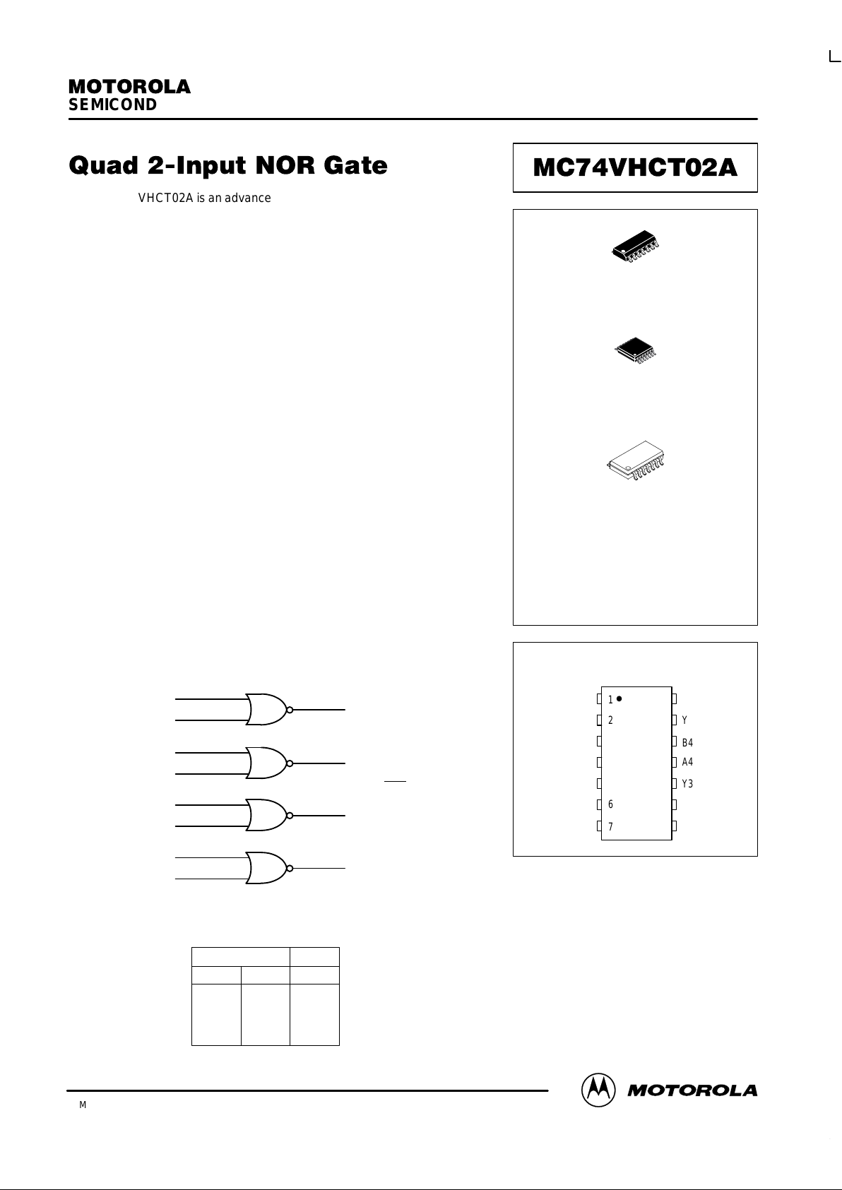
LOGIC DIAGRAM
1
Y1
2
A1
3
B1
Y4
Y = A + B
4
Y2
5
A2
6
B2
10
Y3
8
A3
9
B3
13
11
A4
12
B4
FUNCTION TABLE
A
L
L
H
H
Inputs Output
B
L
H
L
H
Y
H
L
L
L
PIN ASSIGNMENT
11
12
13
14
8
9
105
4
3
2
1
7
6
Y3
A4
B4
Y4
V
CC
A3
B3
Y2
B1
A1
Y1
GND
B2
A2
D SUFFIX
14–LEAD SOIC PACKAGE
CASE 751A–03
DT SUFFIX
14–LEAD TSSOP PACKAGE
CASE 948G–01
ORDERING INFORMATION
MC74VHCTXXAD
MC74VHCTXXADT
MC74VHCTXXAM
SOIC
TSSOP
SOIC EIAJ
M SUFFIX
14–LEAD SOIC EIAJ PACKAGE
CASE 965–01
MC74VHCT02A
MOTOROLA VHC Data – Advanced CMOS Logic
DL203 — Rev 1
2
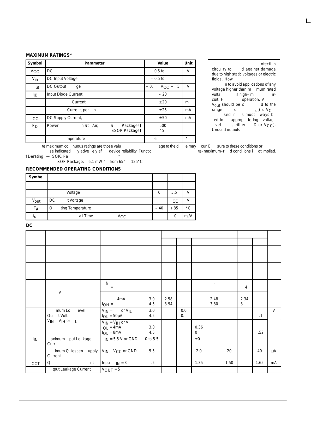
MAXIMUM RATINGS*
Symbol
Parameter
Value
Unit
V
CC
DC Supply Voltage
– 0.5 to + 7.0
V
V
in
DC Input Voltage
– 0.5 to + 7.0
V
V
out
DC Output Voltage
– 0.5 to VCC + 0.5
V
I
IK
Input Diode Current
– 20
mA
I
OK
Output Diode Current
± 20
mA
I
out
DC Output Current, per Pin
± 25
mA
I
CC
DC Supply Current, VCC and GND Pins
± 50
mA
Î
Î
P
D
ОООООООООООО
Î
Power Dissipation in Still Air, SOIC Packages†
TSSOP Package†
ÎÎÎÎ
Î
500
450
Î
Î
mW
T
stg
Storage Temperature
– 65 to + 150
_
C
* Absolute maximum continuous ratings are those values beyond which damage to the device may occur. Exposure to these conditions or conditions
beyond those indicated may adversely affect device reliability. Functional operation under absolute–maximum–rated conditions is not implied.
†Derating — SOIC Packages: – 7 mW/_C from 65_ to 125_C
TSSOP Package: – 6.1 mW/_C from 65_ to 125_C
RECOMMENDED OPERATING CONDITIONS
Symbol
Parameter
Min
Max
Unit
V
CC
DC Supply Voltage
4.5
5.5
V
V
in
DC Input Voltage
0
5.5
V
V
out
DC Output Voltage
0
V
CC
V
T
A
Operating Temperature
– 40
+ 85
_
C
tr, t
f
Input Rise and Fall Time VCC =5.0V ±0.5V
0
20
ns/V
DC ELECTRICAL CHARACTERISTICS
V
TA = 25°C
TA ≤ 85°C
TA ≤ 125°C
Symbol
Parameter
Test Conditions
V
CC
(V)
Min
Typ
Max
Min
Max
Min
Max
Unit
Î
Î
V
IH
ОООООО
Î
Minimum High–Level Input
Voltage
ОООООÎÎ
Î
3.0
4.5
5.5
Î
Î
1.2
2.0
2.0
ÎÎÎÎÎ
Î
1.2
2.0
2.0
ÎÎÎ
Î
1.2
2.0
2.0
ÎÎÎ
V
Î
Î
V
IL
ОООООО
Î
Maximum Low–Level Input
Voltage
ОООООÎÎ
Î
3.0
4.5
5.5
ÎÎÎÎÎ
Î
0.53
0.8
0.8
ÎÎÎ
Î
0.53
0.8
0.8
ÎÎÎ
Î
0.53
0.8
0.8
Î
V
Î
Î
V
OH
ОООООО
Î
Minimum High–Level
Output Voltage
ООООО
Î
VIN = VIH or V
IL
IOH = – 50µA
Î
Î
3.0
4.5
Î
Î
2.9
4.4
Î
Î
3.0
4.5
ÎÎÎ
Î
2.9
4.4
ÎÎÎ
Î
2.9
4.4
ÎÎÎ
V
ÎÎОООООО
Î
VIN = VIH or V
IL
ООООО
Î
VIN = VIH or V
IL
IOH = – 4mA
IOH = – 8mA
Î
Î
3.0
4.5
Î
Î
2.58
3.94
ÎÎÎÎÎ
Î
2.48
3.80
ÎÎÎ
Î
2.34
3.66
ÎÎÎ
Î
V
OL
ОООООО
Maximum Low–Level
Output Voltage
ООООО
VIN = VIH or V
IL
IOL = 50µA
Î
3.0
4.5
Î
Î
0.0
0.0
Î
0.1
0.1
Î
Î
0.1
0.1
Î
Î
0.1
0.1
Î
V
Î
Î
Î
Î
ОООООО
Î
ОООООО
Î
VIN = VIH or V
IL
ООООО
Î
ООООО
Î
VIN = VIH or V
IL
IOL = 4mA
IOL = 8mA
Î
Î
Î
Î
3.0
4.5
Î
Î
Î
Î
Î
Î
Î
Î
Î
Î
Î
Î
0.36
0.36
Î
Î
Î
Î
Î
Î
Î
Î
0.44
0.44
Î
Î
Î
Î
Î
Î
Î
Î
0.52
0.52
Î
Î
I
IN
Maximum Input Leakage
Current
VIN = 5.5 V or GND
0 to 5.5
± 0.1
± 1.0
± 1.0
µA
Î
Î
I
CC
ОООООО
Î
Maximum Quiescent Supply
Current
ООООО
Î
VIN = VCC or GND
Î
Î
5.5
ÎÎÎÎÎ
Î
2.0
ÎÎÎ
Î
20
ÎÎÎ
Î
40εA
I
CCT
Quiescent Supply Current
Input: VIN = 3.4V
5.5
1.35
1.50
1.65
mA
I
OPD
Output Leakage Current
V
OUT
= 5.5V
0.0
0.5
5.0
10
µA
This device contains protection
circuitry to guard against damage
due to high static voltages or electric
fields. However, precautions must
be taken to avoid applications of any
voltage higher than maximum rated
voltages to this high–impedance circuit. For proper operation, Vin and
V
out
should be constrained to the
range GND v (Vin or V
out
) v VCC.
Unused inputs must always be
tied to an appropriate logic voltage
level (e.g., either GND or VCC).
Unused outputs must be left open.
MC74VHCT02A
VHC Data – Advanced CMOS Logic
DL203 — Rev 1
3 MOTOROLA
AC ELECTRICAL CHARACTERISTICS (Input t
r
= tf = 3.0ns)
ОООООООО
TA = 25°C
TA ≤ 85°C
TA ≤ 125°C
Symbol
Parameter
ОООООООО
Test Conditions
Min
Typ
Max
Min
Max
Max
Max
Unit
Î
Î
t
PLH
,
t
PHL
ООООООО
Î
Maximum Propagation
Delay,
ОООООООО
ООООООО
Î
VCC = 3.0 ± 0.3V CL = 15pF
CL = 50pF
ÎÎÎ
Î
5.6
8.1
Î
Î
7.9
11.4
ÎÎÎ
Î
9.5
13.0
ÎÎÎ
Î
12.5
17.5
Î
ns
ÎÎООООООО
Î
Input A or B to Y
ОООООООО
ООООООО
Î
VCC = 5.0 ± 0.5V CL = 15pF
CL = 50pF
ÎÎÎ
Î
3.6
5.1
Î
Î
5.5
7.5
ÎÎÎ
Î
6.5
8.5
ÎÎÎ
Î
9.0
11.0
Î
Î
Î
C
in
ООООООО
Î
Maximum Input Capacitance
ОООООООО
ОООООООÎÎÎÎ
Î
4
Î
Î
10
ÎÎÎ
Î
10
ÎÎÎ
Î
10ÎpF
Typical @ 25°C, VCC = 5.0V
C
PD
Power Dissipation Capacitance (Note 1.)
20
pF
1. CPD is defined as the value of the internal equivalent capacitance which is calculated from the operating current consumption without load.
Average operating current can be obtained by the equation: I
CC(OPR
)
= CPD VCC fin + ICC/4 (per gate). CPD is used to determine the no–load
dynamic power consumption; PD = CPD V
CC
2
fin + ICC VCC.
NOISE CHARACTERISTICS (Input t
r
= tf = 3.0ns, CL = 50pF, VCC = 5.0V)
TA = 25°C
Symbol Characteristic
Typ Max
Unit
V
OLP
Quiet Output Maximum Dynamic V
OL
0.3 0.8 V
V
OLV
Quiet Output Minimum Dynamic V
OL
– 0.3 – 0.8 V
V
IHD
Minimum High Level Dynamic Input Voltage 3.5 V
V
ILD
Maximum Low Level Dynamic Input Voltage 1.5 V
Figure 1. Switching Waveforms
3.0V
GND
1.5V
1.5V
A or B
Y
t
PHL
t
PLH
*Includes all probe and jig capacitance
Figure 2. Test Circuit
CL*
TEST POINT
DEVICE
UNDER
TEST
OUTPUT
V
OH
V
OL
 Loading...