

MOTOROLA MC74VHC595ML2, MC74VHC595M, MC74VHC595D, MC74VHC595DR2, MC74VHC595DT Datasheet
...
SEMICONDUCTOR TECHNICAL DATA
1
REV 1
Motorola, Inc. 1997
6/97
"
! !
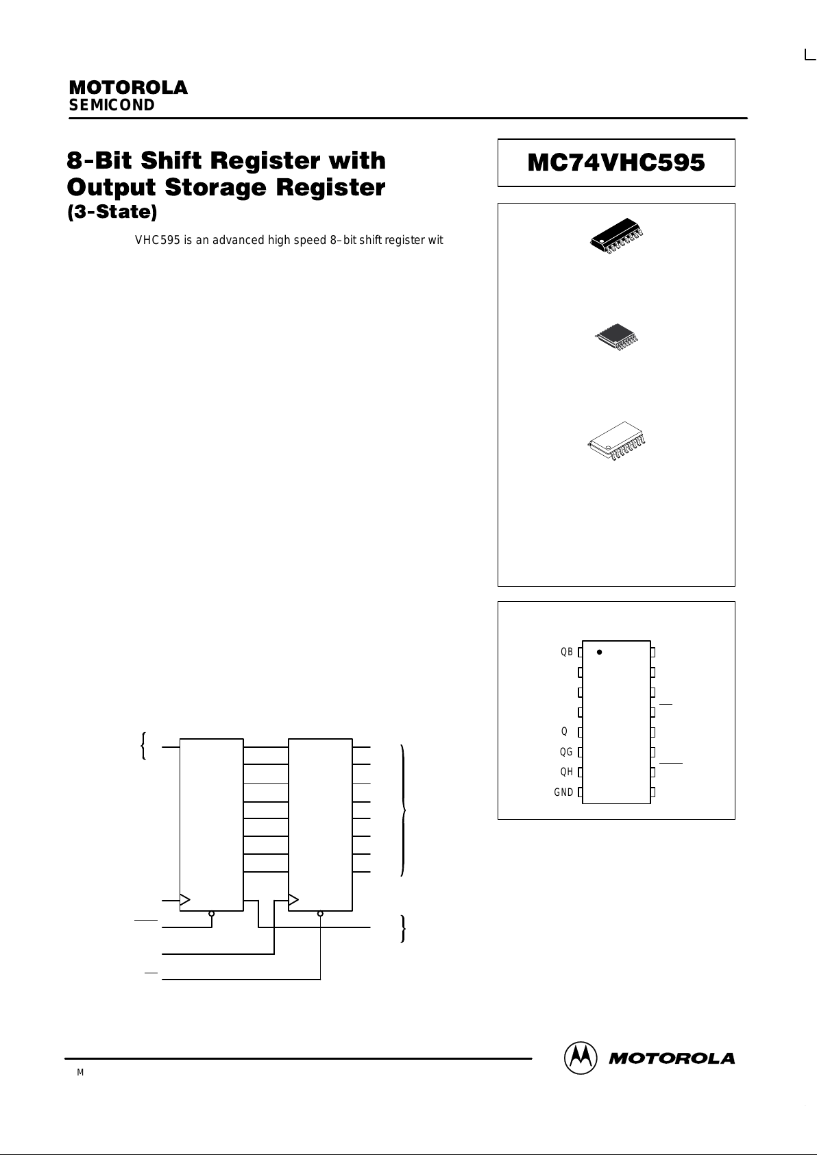
The MC74VHC595 is an advanced high speed 8–bit shift register with an
output storage register fabricated with silicon gate CMOS technology.
It achieves high speed operation similar to equivalent Bipolar Schottky
TTL while maintaining CMOS low power dissipation.
The MC74VHC595 contains an 8–bit static shift register which feeds an
8–bit storage register.
Shift operation is accomplished on the positive going transition of the Shift
Clock input (SCK). The output register is loaded with the contents of the shift
register on the positive going transition of the Register Clock input (RCK).
Since the RCK and SCK signals are independent, parallel outputs can be
held stable during the shift operation. And, since the parallel outputs are
3–state, the VHC595 can be directly connected to an 8–bit bus. This register
can be used in serial–to–parallel conversion, data receivers, etc.
The internal circuit is composed of three stages, including a buffer output
which provides high noise immunity and stable output. The inputs tolerate
voltages up to 7V, allowing the interface of 5V systems to 3V systems.
• High Speed: f
max
= 185MHz (Typ) at VCC = 5V
• Low Power Dissipation: ICC = 4µA (Max) at TA = 25°C
• High Noise Immunity: V
NIH
= V
NIL
= 28% V
CC
• Power Down Protection Provided on Inputs
• Balanced Propagation Delays
• Designed for 2V to 5.5V Operating Range
• Low Noise: V
OLP
= 1.0V (Max)
• Pin and Function Compatible with Other Standard Logic Families
• Latchup Performance Exceeds 300mA
• ESD Performance: HBM > 2000V; Machine Model > 200V
• Chip Complexity: 328 FETs or 82 Equivalent Gates
LOGIC DIAGRAM
SERIAL
DATA
INPUT
14
11
10
12
13
SCK
SCLR
RCK
OE
SHIFT
REGISTER
STORAGE
REGISTER
15
1
2
3
4
5
6
7
9
QA
QB
QC
QD
QE
QF
QG
QH
SQH
SI
PARALLEL
DATA
OUTPUTS
SERIAL
DATA
OUTPUT
PIN ASSIGNMENT
13
14
15
16
9
10
11
125
4
3
2
1
8
7
6
RCK
OE
SI
QA
VCC
SQH
SCLR
SCK
QE
QD
QC
QB
GND
QH
QG
QF
D SUFFIX
16–LEAD SOIC PACKAGE
CASE 751B–05
DT SUFFIX
16–LEAD TSSOP PACKAGE
CASE 948F–01
ORDERING INFORMATION
MC74VHCXXXD
MC74VHCXXXDT
MC74VHCXXXM
SOIC
TSSOP
SOIC EIAJ
M SUFFIX
16–LEAD SOIC EIAJ PACKAGE
CASE 966–01
MC74VHC595
MOTOROLA VHC Data – Advanced CMOS Logic
DL203 — Rev 1
2
FUNCTION TABLE
Inputs Resulting Function
Operation
Reset
(SCLR
)
Serial
Input
(SI)
Shift
Clock
(SCK)
Reg
Clock
(RCK)
Output
Enable
(OE
)
Shift
Register
Contents
Storage
Register
Contents
Serial
Output
(SQH)
Parallel
Outputs
(QA – QH)
Clear shift register L X X L, H, ↓ L L U L U
Shift data into shift register H D ↑ L, H, ↓ L D→SRA;
SRN→SR
N+1
U SRG→SR
H
U
Registers remains
unchanged
H X L, H, ↓ X L U ** U **
Transfer shift register
contents to storage register
H X L, H, ↓ ↑ L U SRN³
STR
N
* SR
N
Storage register remains
unachanged
X X X L, H, ↓ L * U * U
Enable parallel outputs X X X X L * ** * Enabled
Force outputs into high
impedance state
X X X X H * ** * Z
SR = shift register contents D = data (L, H) logic level ↓ = High–to–Low * = depends on Reset and Shift Clock inputs
STR = storage register contents U = remains unchanged ↑ = Low–to–High ** = depends on Register Clock input
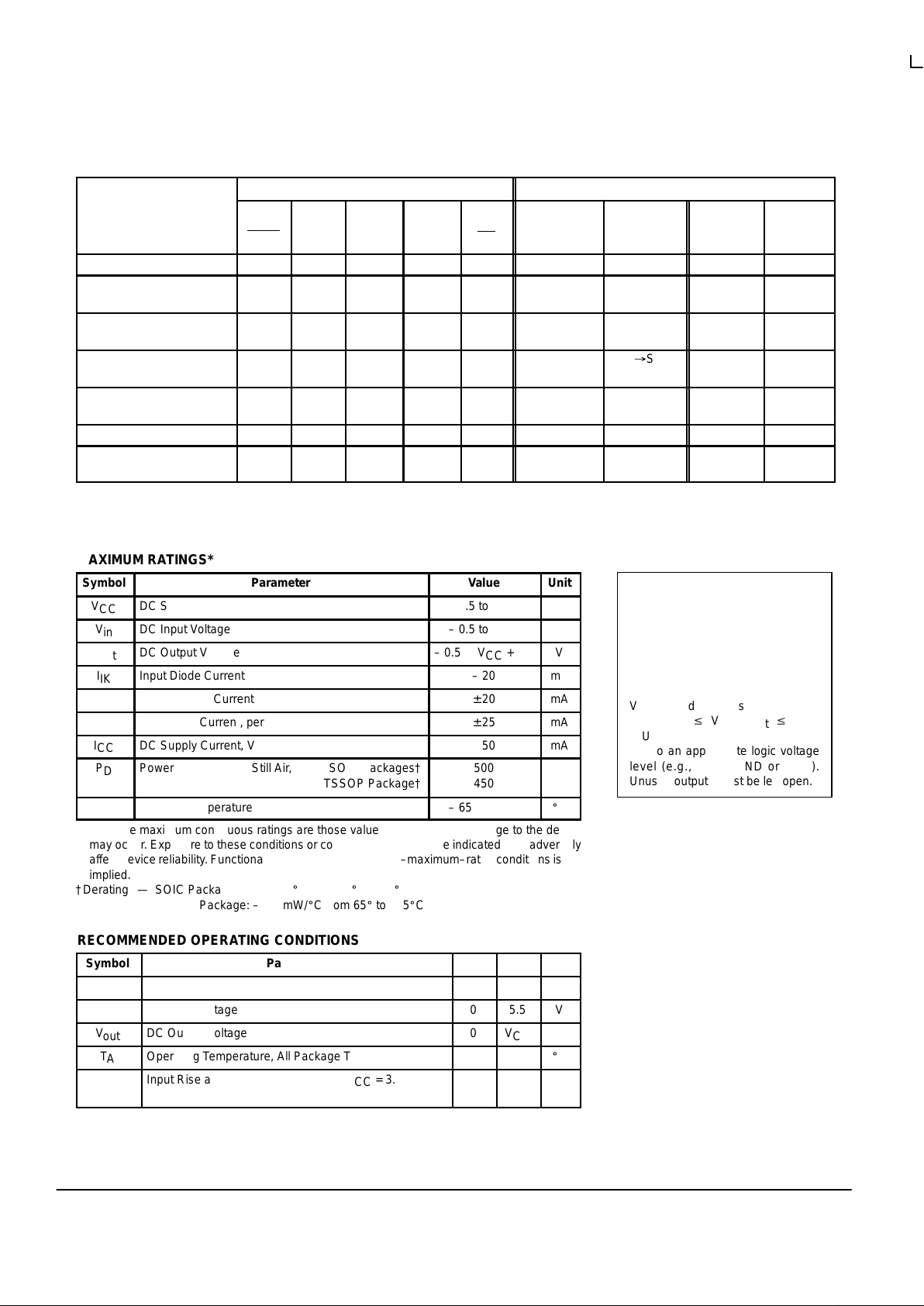
MAXIMUM RATINGS*
Symbol
Parameter
Value
Unit
V
CC
DC Supply Voltage
– 0.5 to + 7.0
V
V
in
DC Input Voltage
– 0.5 to + 7.0
V
V
out
DC Output Voltage
– 0.5 to VCC + 0.5
V
I
IK
Input Diode Current
– 20
mA
I
OK
Output Diode Current
± 20
mA
I
out
DC Output Current, per Pin
± 25
mA
I
CC
DC Supply Current, VCC and GND Pins
± 50
mA
Î
Î
P
D
ОООООООООООО
Î
Power Dissipation in Still Air, SOIC Packages†
TSSOP Package†
ÎÎÎÎ
Î
500
450
Î
Î
mW
T
stg
Storage Temperature
– 65 to + 150
_
C
* Absolute maximum continuous ratings are those values beyond which damage to the device
may occur. Exposure to these conditions or conditions beyond those indicated may adversely
affect device reliability . Functional operation under absolute–maximum–rated conditions is not
implied.
†Derating — SOIC Packages: – 7 mW/_C from 65_ to 125_C
TSSOP Package: – 6.1 mW/_C from 65_ to 125_C
RECOMMENDED OPERATING CONDITIONS
Symbol
Parameter
Min
Max
Unit
V
CC
DC Supply Voltage
2.0
5.5
V
V
in
DC Input Voltage
0
5.5
V
V
out
DC Output Voltage
0
V
CC
V
T
A
Operating Temperature, All Package Types
– 40
+ 85
_
C
tr, t
f
Input Rise and Fall Time VCC = 3.3V ±0.3V
VCC =5.0V ±0.5V00
10020ns/V
This device contains protection
circuitry to guard against damage
due to high static voltages or electric
fields. However, precautions must
be taken to avoid applications of any
voltage higher than maximum rated
voltages to this high–impedance circuit. For proper operation, Vin and
V
out
should be constrained to the
range GND v (Vin or V
out
) v VCC.
Unused inputs must always be
tied to an appropriate logic voltage
level (e.g., either GND or VCC).
Unused outputs must be left open.
MC74VHC595
VHC Data – Advanced CMOS Logic
DL203 — Rev 1
3 MOTOROLA
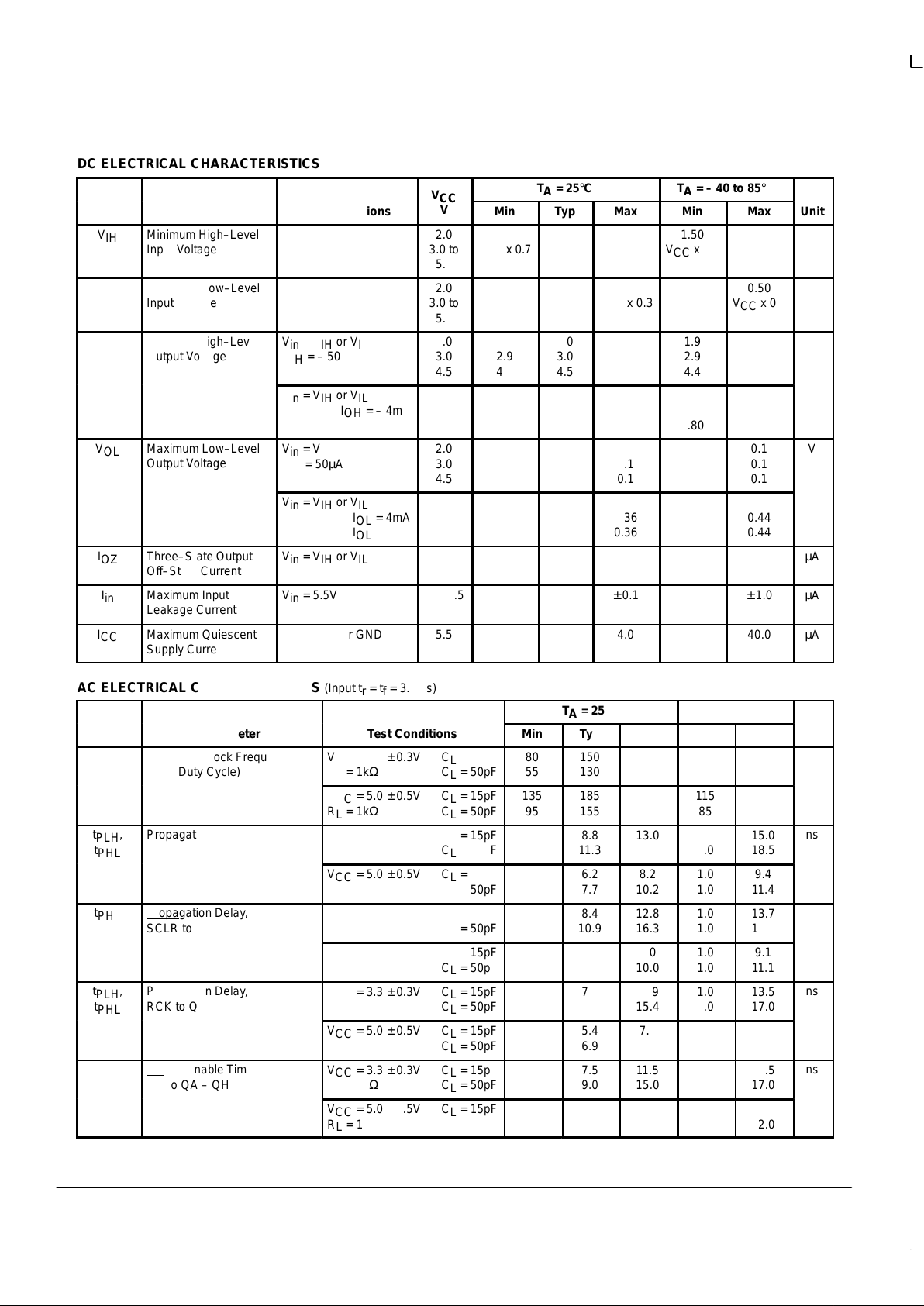
DC ELECTRICAL CHARACTERISTICS
ÎÎÎ
V
TA = 25°C
TA = – 40 to 85°C
Symbol
Parameter
Test Conditions
ÎÎÎ
V
CC
V
Min
Typ
Max
Min
Max
Unit
ÎÎ
Î
ÎÎ
Î
V
IH
ÎÎÎÎ
Î
ÎÎÎÎ
Î
Minimum High–Level
Input Voltage
ОООООО
Î
ОООООО
Î
ÎÎÎ
ÎÎ
Î
ÎÎ
Î
2.0
3.0 to
5.5
ÎÎ
Î
ÎÎ
Î
1.50
VCC x 0.7
Î
Î
Î
Î
ÎÎ
Î
ÎÎ
Î
ÎÎ
Î
ÎÎ
Î
1.50
VCC x 0.7
ÎÎ
Î
ÎÎ
Î
V
ÎÎ
Î
ÎÎ
Î
V
IL
ÎÎÎÎ
Î
ÎÎÎÎ
Î
Maximum Low–Level
Input Voltage
ОООООО
Î
ОООООО
Î
ÎÎÎ
ÎÎ
Î
ÎÎ
Î
2.0
3.0 to
5.5
ÎÎ
Î
ÎÎ
Î
Î
Î
Î
Î
ÎÎ
Î
ÎÎ
Î
0.50
VCC x 0.3
ÎÎ
Î
ÎÎ
Î
ÎÎ
Î
ÎÎ
Î
0.50
VCC x 0.3
V
ÎÎ
Î
V
OH
ÎÎÎÎ
Î
Minimum High–Level
Output Voltage
ОООООО
Î
Vin = VIH or V
IL
IOH = – 50µA
ÎÎÎ
ÎÎ
Î
2.0
3.0
4.5
ÎÎ
Î
1.9
2.9
4.4
Î
Î
2.0
3.0
4.5
ÎÎÎÎÎ
Î
1.9
2.9
4.4
ÎÎ
Î
V
ÎÎ
Î
ÎÎ
ÎÎÎÎ
Î
ÎÎÎÎ
ОООООО
Î
ОООООО
Vin = VIH or V
IL
IOH = – 4mA
IOH = – 8mA
ÎÎÎ
ÎÎ
Î
ÎÎ
3.0
4.5
ÎÎ
Î
ÎÎ
2.58
3.94
Î
Î
Î
ÎÎ
Î
ÎÎ
ÎÎ
Î
ÎÎ
2.48
3.80
ÎÎ
Î
ÎÎ
ÎÎ
Î
ÎÎ
Î
V
OL
ÎÎÎÎ
Î
ÎÎÎÎ
Î
Maximum Low–Level
Output Voltage
ОООООО
Î
ОООООО
Î
Vin = VIH or V
IL
IOL = 50µA
ÎÎÎ
ÎÎ
Î
ÎÎ
Î
2.0
3.0
4.5
ÎÎ
Î
ÎÎ
Î
Î
Î
Î
Î
0.0
0.0
0.0
ÎÎ
Î
ÎÎ
Î
0.1
0.1
0.1
ÎÎ
Î
ÎÎ
Î
ÎÎ
Î
ÎÎ
Î
0.1
0.1
0.1
V
ÎÎÎÎÎÎÎÎОООООО
Î
Vin = VIH or V
IL
IOL = 4mA
IOL = 8mA
ÎÎÎ
ÎÎ
Î
3.0
4.5
ÎÎÎÎÎÎÎ
Î
0.36
0.36
ÎÎÎÎÎ
Î
0.44
0.44
ÎÎ
Î
I
OZ
ÎÎÎÎ
Î
Three–State Output
Off–State Current
ОООООО
Î
Vin = VIH or V
IL
V
out
= VCC or GND
ÎÎÎ
ÎÎ
Î
5.5
ÎÎÎÎÎÎÎ
Î
± 0.25
ÎÎÎÎÎ
Î
± 2.50
µA
ÎÎ
I
in
ÎÎÎÎ
Maximum Input
Leakage Current
ОООООО
Vin = 5.5V or GND
ÎÎÎ
ÎÎ
0 to 5.5
ÎÎ
Î
ÎÎ
± 0.1
ÎÎ
ÎÎ
± 1.0
µA
ÎÎ
Î
I
CC
ÎÎÎÎ
Î
Maximum Quiescent
Supply Current
ОООООО
Î
Vin = VCC or GND
ÎÎÎ
ÎÎ
Î
5.5
ÎÎÎÎÎÎÎ
Î
4.0
ÎÎÎÎÎ
Î
40.0
µA
AC ELECTRICAL CHARACTERISTICS (Input t
r
= tf = 3.0 ns)
TA = 25°C
TA = – 40 to 85°C
Symbol
Parameter
Test Conditions
Min
Typ
Max
Min
Max
Unit
ÎÎ
f
max
ОООООО
Maximum Clock Frequency
(50% Duty Cycle)
ООООООО
VCC = 3.3 ± 0.3V CL = 15pF
RL = 1kΩ CL = 50pF
ÎÎ
80
55
Î
150
130
ÎÎ
Î
70
50
ÎÎ
MHz
ÎÎÎООООООÎООООООО
Î
VCC = 5.0 ± 0.5V CL = 15pF
RL = 1kΩ CL = 50pF
ÎÎ
Î
135
95
Î
Î
185
155
ÎÎÎÎ
Î
115
85
ÎÎ
Î
ÎÎ
Î
t
PLH
,
t
PHL
ОООООО
Î
Propagation Delay,
SCK to SQH
ООООООО
Î
VCC = 3.3 ± 0.3V CL = 15pF
CL = 50pF
ÎÎÎÎ
Î
8.8
11.3
ÎÎ
Î
13.0
16.5
Î
Î
1.0
1.0
ÎÎ
Î
15.0
18.5
ns
ÎÎÎООООООÎООООООО
Î
VCC = 5.0 ± 0.5V CL = 15pF
CL = 50pF
ÎÎÎÎ
Î
6.2
7.7
ÎÎ
Î
8.2
10.2
Î
Î
1.0
1.0
ÎÎ
Î
9.4
11.4
ÎÎ
Î
t
PHL
ОООООО
Î
Propagation Delay,
SCLR
to SQH
ООООООО
Î
VCC = 3.3 ± 0.3V CL = 15pF
CL = 50pF
ÎÎÎÎ
Î
8.4
10.9
ÎÎ
Î
12.8
16.3
Î
Î
1.0
1.0
ÎÎ
Î
13.7
17.2
ns
ÎÎÎООООООÎООООООО
Î
VCC = 5.0 ± 0.5V CL = 15pF
CL = 50pF
ÎÎÎÎ
Î
5.9
7.4
ÎÎ
Î
8.0
10.0
Î
Î
1.0
1.0
ÎÎ
Î
9.1
11.1
ÎÎ
Î
t
PLH
,
t
PHL
ОООООО
Î
Propagation Delay,
RCK to QA – QH
ООООООО
Î
VCC = 3.3 ± 0.3V CL = 15pF
CL = 50pF
ÎÎÎÎ
Î
7.7
10.2
ÎÎ
Î
11.9
15.4
Î
Î
1.0
1.0
ÎÎ
Î
13.5
17.0
ns
VCC = 5.0 ± 0.5V CL = 15pF
CL = 50pF
5.4
6.9
7.4
9.4
1.0
1.0
8.5
10.5
ÎÎ
Î
t
PZL
,
t
PZH
ОООООО
Î
Output Enable Time,
OE
to QA – QH
ООООООО
Î
VCC = 3.3 ± 0.3V CL = 15pF
RL = 1kΩ CL = 50pF
ÎÎÎÎ
Î
7.5
9.0
ÎÎ
Î
11.5
15.0
Î
Î
1.0
1.0
ÎÎ
Î
13.5
17.0
ns
ÎÎÎООООООÎООООООО
Î
VCC = 5.0 ± 0.5V CL = 15pF
RL = 1kΩ CL = 50pF
ÎÎÎÎ
Î
4.8
8.3
ÎÎ
Î
8.6
10.6
Î
Î
1.0
1.0
ÎÎ
Î
10.0
12.0
 Loading...