

MOTOROLA MC74VHC393ML1, MC74VHC393ML2, MC74VHC393M, MC74VHC393MEL, MC74VHC393D Datasheet
...
SEMICONDUCTOR TECHNICAL DATA
1
REV 0
Motorola, Inc. 1997
6/97
The MC74VHC393 is an advanced high speed CMOS dual 4–bit binary
ripple counter fabricated with silicon gate CMOS technology . It achieves high
speed operation similar to equivalent Bipolar Schottky TTL while maintaining
CMOS low power dissipation.
This device consists of two independent 4–bit binary ripple counters with
parallel outputs from each counter stage. A ÷256 counter can be obtained by
cascading the two binary counters.
Internal flip–flops are triggered by high–to–low transitions of the clock
input. Reset for the counters is asynchronous and active–high. State
changes of the Q outputs do not occur simultaneously because of internal
ripple delays. Therefore, decoded output signals are subject to decoding
spikes and should not be used as clocks or as strobes except when gated
with the Clock of the VHC393.
The inputs tolerate voltages up to 7V , allowing the interface of 5V systems
to 3V systems.
• High Speed: f
max
= 170MHz (Typ) at VCC = 5V
• Low Power Dissipation: ICC = 4µA (Max) at TA = 25°C
• High Noise Immunity: V
NIH
= V
NIL
= 28% V
CC
• Power Down Protection Provided on Inputs
• Balanced Propagation Delays
• Designed for 2V to 5.5V Operating Range
• Low Noise: V
OLP
= 0.8V (Max)
• Pin and Function Compatible with Other Standard Logic Families
• Latchup Performance Exceeds 300mA
• ESD Performance: HBM > 2000V; Machine Model > 200V
• Chip Complexity: 236 FETs or 59 Equivalent Gates
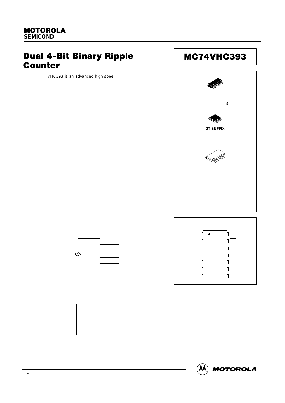
LOGIC DIAGRAM
nQA
nQB
nQC
nQD
CPn
RDn
1, 13
2, 12
3, 11
4, 10
5, 9
6, 8
BINARY
COUNTER
FUNCTION TABLE
Inputs
Clock Reset Outputs
XH L
H L No Change
L L No Change
↑ L No Change
↓ L Next State
D SUFFIX
14–LEAD SOIC PACKAGE
CASE 751A–03
DT SUFFIX
14–LEAD TSSOP PACKAGE
CASE 948G–01
ORDERING INFORMATION
MC74VHCXXXD
MC74VHCXXXDT
MC74VHCXXXM
SOIC
TSSOP
SOIC EIAJ
M SUFFIX
14–LEAD SOIC EIAJ PACKAGE
CASE 965–01
PIN ASSIGNMENT
11
12
13
14
8
9
105
4
3
2
1
7
6
2QB
2QA
RD2
CP2
V
CC
2QD
2QC
1QB
1QA
RD1
CP1
GND
1QC
1QD
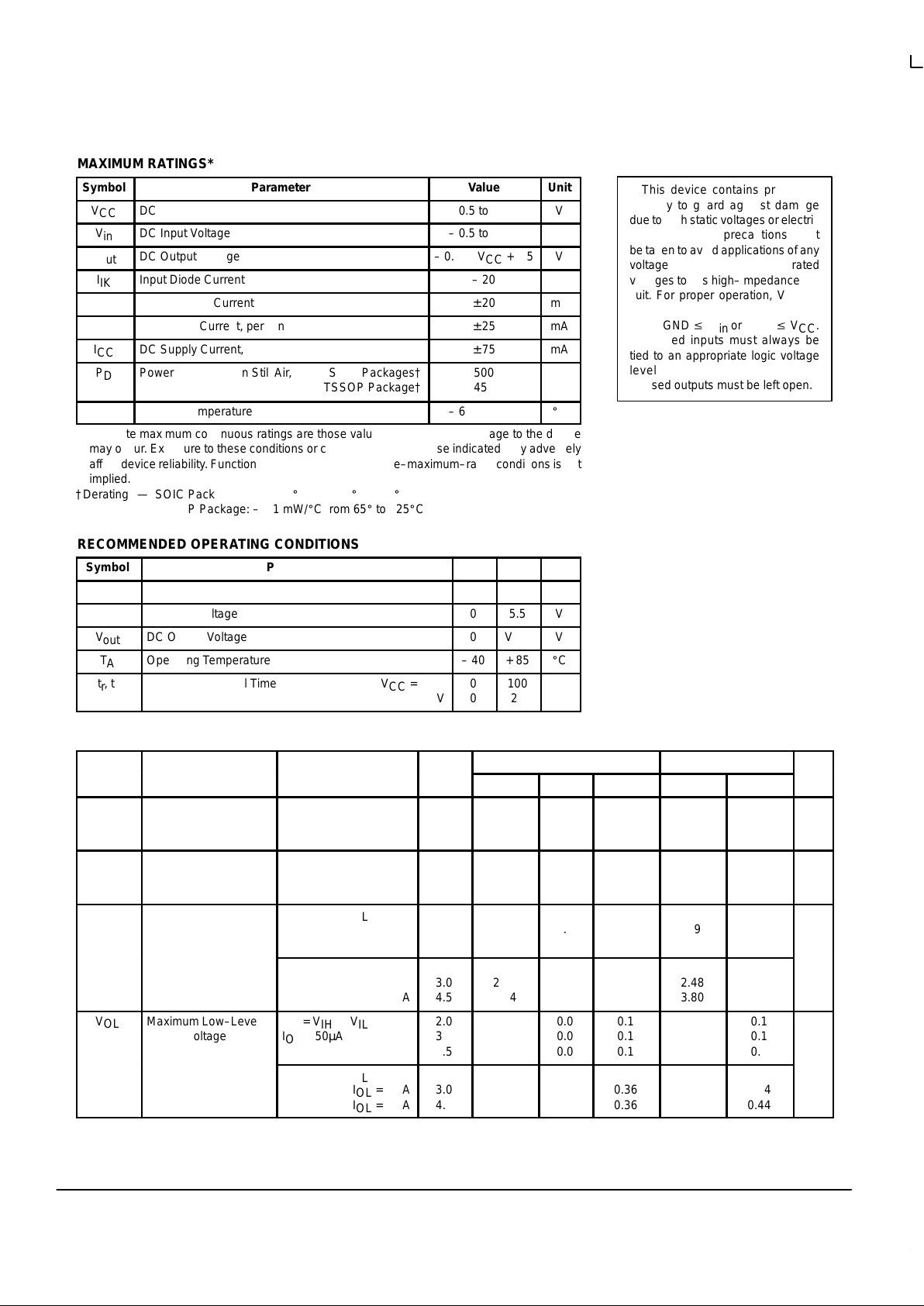
MC74VHC393
MOTOROLA VHC Data – Advanced CMOS Logic
DL203 — Rev 1
2
MAXIMUM RATINGS*
Symbol
Parameter
Value
Unit
V
CC
DC Supply Voltage
– 0.5 to + 7.0
V
V
in
DC Input Voltage
– 0.5 to + 7.0
V
V
out
DC Output Voltage
– 0.5 to VCC + 0.5
V
I
IK
Input Diode Current
– 20
mA
I
OK
Output Diode Current
± 20
mA
I
out
DC Output Current, per Pin
± 25
mA
I
CC
DC Supply Current, VCC and GND Pins
± 75
mA
Î
Î
P
D
ОООООООООООО
Î
Power Dissipation in Still Air, SOIC Packages†
TSSOP Package†
ÎÎÎÎ
Î
500
450
Î
Î
mW
T
stg
Storage Temperature
– 65 to + 150
_
C
* Absolute maximum continuous ratings are those values beyond which damage to the device
may occur. Exposure to these conditions or conditions beyond those indicated may adversely
affect device reliability . Functional operation under absolute–maximum–rated conditions is not
implied.
†Derating — SOIC Packages: – 7 mW/_C from 65_ to 125_C
TSSOP Package: – 6.1 mW/_C from 65_ to 125_C
RECOMMENDED OPERATING CONDITIONS
Symbol
Parameter
Min
Max
Unit
V
CC
DC Supply Voltage
2.0
5.5
V
V
in
DC Input Voltage
0
5.5
V
V
out
DC Output Voltage
0
V
CC
V
T
A
Operating Temperature
– 40
+ 85
_
C
tr, t
f
Input Rise and Fall Time VCC = 3.3V
VCC = 5.0V00
10020ns/V
DC ELECTRICAL CHARACTERISTICS
ÎÎÎ
V
TA = 25°C
TA = – 40 to 85°C
Symbol
Parameter
Test Conditions
ÎÎÎ
V
CC
V
Min
Typ
Max
Min
Max
Unit
ÎÎ
Î
V
IH
ÎÎÎÎ
Î
Minimum High–Level
Input Voltage
ОООООО
Î
ÎÎÎ
ÎÎ
Î
2.0
3.0 to
5.5
ÎÎ
Î
1.50
VCC x 0.7
ÎÎÎÎÎÎÎ
Î
1.50
VCC x 0.7
ÎÎ
Î
V
ÎÎ
Î
ÎÎ
Î
V
IL
ÎÎÎÎ
Î
ÎÎÎÎ
Î
Maximum Low–Level
Input Voltage
ОООООО
Î
ОООООО
Î
ÎÎÎ
ÎÎ
Î
ÎÎ
Î
2.0
3.0 to
5.5
ÎÎ
Î
ÎÎ
Î
Î
Î
Î
Î
ÎÎ
Î
ÎÎ
Î
0.50
VCC x 0.3
ÎÎ
Î
ÎÎ
Î
ÎÎ
Î
ÎÎ
Î
0.50
VCC x 0.3
V
ÎÎ
Î
ÎÎ
Î
V
OH
ÎÎÎÎ
Î
ÎÎÎÎ
Î
Minimum High–Level
Output Voltage
ОООООО
Î
ОООООО
Î
Vin = VIH or V
IL
IOH = – 50µA
ÎÎÎ
ÎÎ
Î
ÎÎ
Î
2.0
3.0
4.5
ÎÎ
Î
ÎÎ
Î
1.9
2.9
4.4
Î
Î
Î
Î
2.0
3.0
4.5
ÎÎ
Î
ÎÎ
Î
ÎÎ
Î
ÎÎ
Î
1.9
2.9
4.4
ÎÎ
Î
ÎÎ
Î
V
ÎÎÎÎÎÎÎÎОООООО
Î
Vin = VIH or V
IL
IOH = – 4mA
IOH = – 8mA
ÎÎÎ
ÎÎ
Î
3.0
4.5
ÎÎ
Î
2.58
3.94
ÎÎÎÎÎÎÎ
Î
2.48
3.80
ÎÎ
Î
ÎÎ
Î
ÎÎ
V
OL
ÎÎÎÎ
Î
ÎÎÎÎ
Maximum Low–Level
Output Voltage
ОООООО
Î
ОООООО
Vin = VIH or V
IL
IOL = 50µA
ÎÎÎ
ÎÎ
Î
ÎÎ
2.0
3.0
4.5
ÎÎ
Î
ÎÎ
Î
Î
Î
0.0
0.0
0.0
ÎÎ
Î
ÎÎ
0.1
0.1
0.1
ÎÎ
Î
ÎÎ
ÎÎ
Î
ÎÎ
0.1
0.1
0.1
V
ÎÎ
Î
ÎÎ
Î
ÎÎÎÎ
Î
ÎÎÎÎ
Î
ОООООО
Î
ОООООО
Î
Vin = VIH or V
IL
IOL = 4mA
IOL = 8mA
ÎÎÎ
ÎÎ
Î
ÎÎ
Î
3.0
4.5
ÎÎ
Î
ÎÎ
Î
Î
Î
Î
Î
ÎÎ
Î
ÎÎ
Î
0.36
0.36
ÎÎ
Î
ÎÎ
Î
ÎÎ
Î
ÎÎ
Î
0.44
0.44
This device contains protection
circuitry to guard against damage
due to high static voltages or electric
fields. However, precautions must
be taken to avoid applications of any
voltage higher than maximum rated
voltages to this high–impedance circuit. For proper operation, Vin and
V
out
should be constrained to the
range GND v (Vin or V
out
) v VCC.
Unused inputs must always be
tied to an appropriate logic voltage
level (e.g., either GND or VCC).
Unused outputs must be left open.
MC74VHC393
VHC Data – Advanced CMOS Logic
DL203 — Rev 1
3 MOTOROLA
DC ELECTRICAL CHARACTERISTICS
Unit
TA = – 40 to 85°C
TA = 25°C
ÎÎÎ
V
CC
V
Test Conditions
Parameter
Symbol
Unit
Max
Min
Max
Typ
Min
ÎÎÎ
V
CC
V
Test Conditions
Parameter
Symbol
ÎÎ
Î
I
in
ÎÎÎÎ
Î
Maximum Input
Leakage Current
ОООООО
Î
Vin = 5.5V or GND
ÎÎÎ
ÎÎ
Î
0 to 5.5
ÎÎÎÎÎÎÎ
Î
± 0.1
ÎÎÎÎÎ
Î
± 1.0
µA
ÎÎ
Î
I
CC
ÎÎÎÎ
Î
Maximum Quiescent
Supply Current
ОООООО
Î
Vin = VCC or GND
ÎÎÎ
ÎÎ
Î
5.5
ÎÎÎÎÎÎÎ
Î
4.0
ÎÎÎÎÎ
Î
40.0
µA
AC ELECTRICAL CHARACTERISTICS (Input t
r
= tf = 3.0ns)
TA = 25°C
TA = – 40 to 85°C
Symbol
Parameter
Test Conditions
Min
Typ
Max
Min
Max
Unit
ÎÎ
Î
f
max
ОООООО
Î
Maximum Clock Frequency
(50% Duty Cycle)
ООООООО
Î
VCC = 3.3 ± 0.3V CL = 15pF
CL = 50pF
ÎÎ
Î
75
45
Î
Î
120
65
ÎÎÎÎ
Î
65
35
ÎÎ
Î
ns
ÎÎÎООООООÎООООООО
Î
VCC = 5.0 ± 0.5V CL = 15pF
CL = 50pF
ÎÎ
Î
125
85
Î
Î
170
115
ÎÎÎÎ
Î
105
75
ÎÎ
Î
t
PLH
,
t
PHL
Maximum Propagation Delay,
CP
to QA
VCC = 3.3 ± 0.3V CL = 15pF
CL = 50pF
8.6
11.1
13.2
16.7
1.0
1.0
15.5
19.0
ns
ÎÎÎООООООÎООООООО
Î
VCC = 5.0 ± 0.5V CL = 15pF
CL = 50pF
ÎÎÎÎ
Î
5.8
7.3
ÎÎ
Î
8.5
10.5
Î
Î
1.0
1.0
ÎÎ
Î
10.0
12.0
ÎÎ
Î
t
PLH
,
t
PHL
ОООООО
Î
Maximum Propagation Delay,
CP
to QB
ООООООО
Î
VCC = 3.3 ± 0.3V CL = 15pF
CL = 50pF
ÎÎÎÎ
Î
10.2
12.7
ÎÎ
Î
15.8
19.3
Î
Î
1.0
1.0
ÎÎ
Î
18.5
22.0
ns
VCC = 5.0 ± 0.5V CL = 15pF
CL = 50pF
6.8
8.3
9.8
11.8
1.0
1.0
11.5
13.5
ÎÎ
Î
t
PLH
,
t
PHL
ОООООО
Î
Maximum Propagation Delay,
CP
to QC
ООООООО
Î
VCC = 3.3 ± 0.3V CL = 15pF
CL = 50pF
ÎÎÎÎ
Î
11.7
14.2
ÎÎ
Î
18.0
21.5
Î
Î
1.0
1.0
ÎÎ
Î
21.0
24.5
ns
ÎÎÎООООООÎООООООО
Î
VCC = 5.0 ± 0.5V CL = 15pF
CL = 50pF
ÎÎÎÎ
Î
7.7
9.2
ÎÎ
Î
11.2
13.2
Î
Î
1.0
1.0
ÎÎ
Î
13.0
15.0
t
PLH
,
t
PHL
Maximum Propagation Delay,
CP
to QD
VCC = 3.3 ± 0.3V CL = 15pF
CL = 50pF
13.0
15.5
19.7
23.2
1.0
1.0
23.0
26.5
ns
ÎÎÎООООООÎООООООО
Î
VCC = 5.0 ± 0.5V CL = 15pF
CL = 50pF
ÎÎÎÎ
Î
8.5
10.0
ÎÎ
Î
12.5
14.5
Î
Î
1.0
1.0
ÎÎ
Î
14.5
16.5
ÎÎ
Î
t
PHL
ОООООО
Î
Maximum Propagation Delay,
RD to Qn
ООООООО
Î
VCC = 3.3 ± 0.3V CL = 15pF
CL = 50pF
ÎÎÎÎ
Î
7.9
10.4
ÎÎ
Î
12.3
15.8
Î
Î
1.0
1.0
ÎÎ
Î
14.5
18.0
ns
ÎÎ
ОООООО
ООООООО
VCC = 5.0 ± 0.5V CL = 15pF
CL = 50pF
ÎÎ
Î
5.4
6.9
ÎÎ
8.1
10.1
Î
1.0
1.0
ÎÎ
9.5
11.5
ÎÎ
Î
t
OSLH
,
t
OSHL
ОООООО
Î
Output to Output Skew
ООООООО
Î
VCC = 3.3 ± 0.3V CL = 50pF
(Note NO TAG)
ÎÎÎÎÎÎÎ
Î
1.5
ÎÎÎÎ
Î
1.5
pF
ÎÎÎООООООÎООООООО
Î
VCC = 5.0 ± 0.5V CL = 50pF
(Note NO TAG)
ÎÎÎÎÎÎÎ
Î
1.0
ÎÎÎÎ
Î
1.0
pF
C
in
Maximum Input Capacitance
4
10
10
pF
Typical @ 25°C, VCC = 5.0V
C
PD
Power Dissipation Capacitance (Note NO T AG)
23
pF
1. Parameter guaranteed by design. t
OSLH
= |t
PLHm
– t
PLHn
|, t
OSHL
= |t
PHLm
– t
PHLn
|.
2. CPD is defined as the value of the internal equivalent capacitance which is calculated from the operating current consumption without load.
Average operating current can be obtained by the equation: I
CC(OPR
)
= CPD VCC fin + ICC/2 (per 4–bit counter). CPD is used to determine
the no–load dynamic power consumption; PD = CPD V
CC
2
fin + ICC VCC.
 Loading...