

Motorola MC54HCT163AJ, MC74HCT163AN, MC74HCT161AD, MC74HCT161AN, MC74HCT163AD Datasheet
...
SEMICONDUCTOR TECHNICAL DATA
1
REV 2
Motorola, Inc. 1995
10/95
High–Performance Silicon–Gate CMOS
The MC54/74HCT161A and HCT163A are identical in pinout to the LS161A
and LS163A. These devices may be used as level converters for interfacing
TTL or NMOS outputs to high speed CMOS inputs.
The HCT161A and HCT163A are programmable 4–bit binary counters with
asynchronous and synchronous reset, respectively.
• Output Drive Capability: 10 LSTTL Loads
• TTL, NMOS Compatible Input Levels
• Outputs Directly Interface to CMOS, NMOS, and TTL
• Operating Voltage Range: 4.5 to 5.5 V
• Low Input Current: 1 µA
• High Noise Immunity Characteristic of CMOS Devices
• In Compliance with the Requirements Defined by JEDEC Standard
No. 7A
• Chip Complexity: 200 FETs or 50 Equivalent Gates
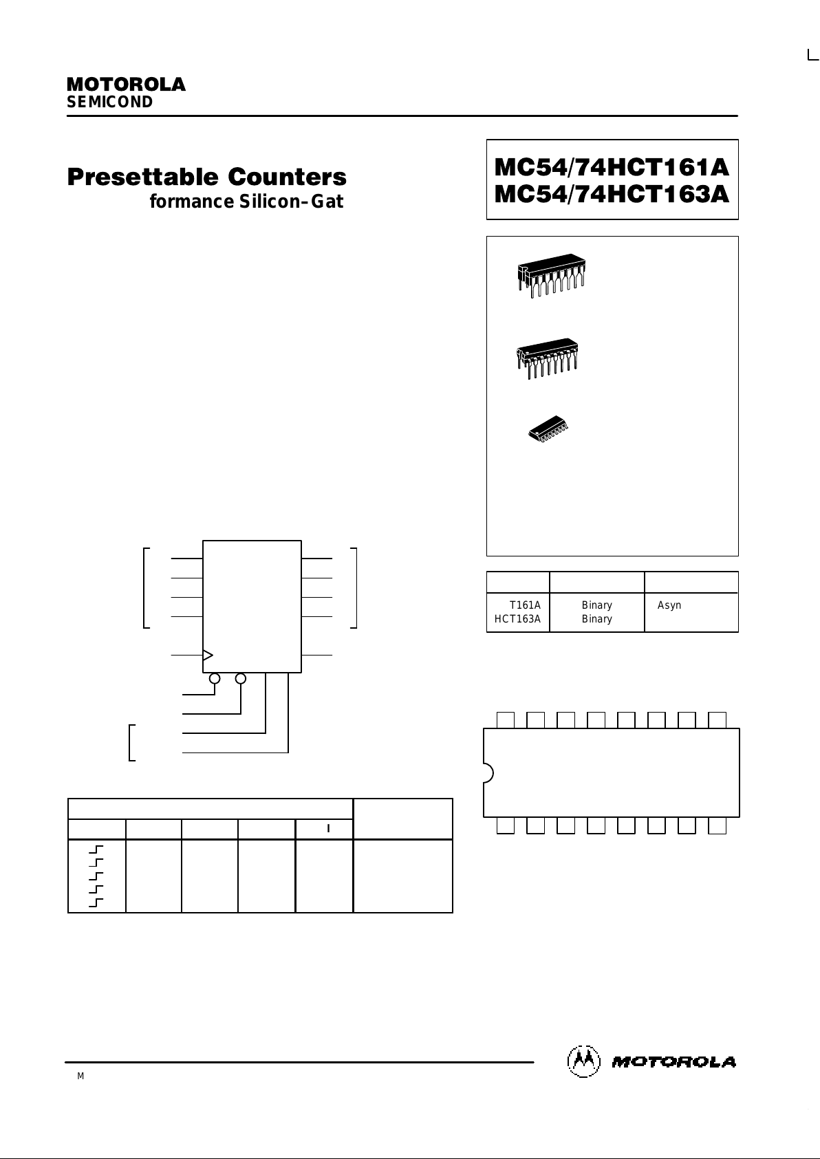
LOGIC DIAGRAM
Reset
Preset
Data
Inputs
Pin 16 = VCC
Pin 8 = GND
1
P
3
6
P
2
5
P
1
4
P
0
3
Clock
2
Q
3
11
Q
2
12
Q
1
13
Q
0
14
Reset
1
Load
9
Enable P
7
Enable T
10
BCD or Binary
Outputs
Count
Enables
Ripple
Carry Out
15
FUNCTION TABLE
Inputs
Clock Reset* Load Enable P Enable T
Output
Q
L
H
H
H
H
X
L
H
H
H
X
X
H
L
X
X
X
H
X
L
Reset
Load Preset Data
Count
No Count
No Count
H = High Level; L = Low Level; X = Don’t Care
* = HCT163A only. HCT161A is an “Asynchronous–Reset” device.
Device Count Mode Reset Mode
HCT161A
HCT163A
Binary
Binary
Asynchronous
Synchronous
D SUFFIX
SOIC PACKAGE
CASE 751B–05
N SUFFIX
PLASTIC PACKAGE
CASE 648–08
ORDERING INFORMATION
MC54HCXXXAJ
MC74HCXXXAN
MC74HCXXXAD
Ceramic
Plastic
SOIC
1
16
1
16
J SUFFIX
CERAMIC PACKAGE
CASE 620–10
1
16
Pinout: 16–Lead Package (Top View)
1516 14 13 12 11 10
21 3 4 5 6 7
V
CC
9
8
RCO* Q0Q1Q2Q
3
Enable
T
Load
Reset Clock P0P1P2P3EnablePGND
* RCO = Ripple Carry Out

MC54/74HCT161A MC54/74HCT163A
MOTOROLA High–Speed CMOS Logic Data
DL129 — Rev 6
2
MAXIMUM RATINGS*
Symbol
Parameter
Value
Unit
V
CC
Positive DC Supply Voltage (Referenced to GND)
– 0.5 to + 7.0
V
V
in
DC Input Voltage (Referenced to GND)
– 1.5 to VCC + 1.5
V
V
out
DC Output Voltage (Referenced to GND)
– 0.5 to VCC + 0.5
V
I
in
DC Input Current, per Pin
± 20
mA
I
out
DC Output Current, per Pin
± 25
mA
I
CC
DC Supply Current, VCC and GND Pins
± 50
mA
P
D
Power Dissipation in Still Air,Plastic or Ceramic DIP†
SOIC Package†
750
500
mW
T
stg
Storage Temperature Range
– 65 to + 150
_
C
T
L
Lead Temperature, 1 mm from Case for 10 Seconds
Plastic DIP or SOIC Package
Ceramic DIP
260
300
_
C
*Maximum Ratings are those values beyond which damage to the device may occur.
Functional operation should be restricted to the Recommended Operating Conditions.
†Derating — Plastic DIP: – 10 mW/_C from 65_ to 125_C
Ceramic DIP: – 10 mW/_C from 100_ to 125_C
SOIC Package: – 7 mW/_C from 65_ to 125_C
For high frequency or heavy load considerations, see Chapter 2 of the Motorola High–Speed CMOS Data Book (DL129/D).
RECOMMENDED OPERATING CONDITIONS
Symbol
Parameter
Min
Max
Unit
V
CC
DC Supply Voltage (Referenced to GND)
4.5
5.5
V
Vin, V
out
DC Input Voltage, Output Voltage (Referenced to GND)
0
V
CC
V
T
A
Operating Temperature, All Package Types
– 55
+ 125
_
C
tr, t
f
Input Rise and Fall Time (Figure 1)
0
500
ns
DC ELECTRICAL CHARACTERISTICS (Voltages referenced to GND)
V
CC
Guaranteed Limit
Symbol Parameter Test Conditions V
– 55 to 25_C
≤ 85°C ≤ 125°C Unit
V
IH
Minimum High–Level Input
Voltage
V
out
= 0.1 V or VCC = –1.0V
|I
out
| v 20 µA
4.5
5.5
2.0
2.0
2.0
2.0
2.0
2.0
V
V
IL
Maximum Low–Level Input
Voltage
V
out
= 0.1 V
|I
out
| v 20 µA
4.5
5.5
0.80
0.80
0.80
0.80
0.80
0.80
V
V
OH
Minimum High–Level Output
Voltage
Vin = VIH or V
IL
|I
out
| v 20 µA
4.5
5.5
4.4
5.4
4.4
5.4
4.4
5.4
V
Vin = VIH or V
IL
|I
out
| v 4.0 mA
4.5 3.98 3.84 3.70 V
V
OL
Maximum Low–Level Output
Voltage
Vin = VIH or V
IL
|I
out
| v 20 µA
4.5
5.5
0.10
0.10
0.10
0.10
0.10
0.10
V
Vin = VIH or V
IL
|I
out
| v 4.0 mA
4.5 0.26 0.33 0.40 V
I
in
Maximum Input Leakage Current Vin = VCC or GND 5.5 ± 0.10 ± 1.00 ± 1.00 µA
I
CC
Maximum Quiescent Supply
Current (Per Package)
Vin = VCC or GND
I
out
– 0 µA
5.5 4 40 160 µA
I
CC
Additional Quiescent Supply
Vin = 2.4V,
Any One Input
≥–55°C 25 to +125°C
ICCAdditional Quiescent Supply
Current
Any One Input
VIN = VCC or GND
Other Inputs I
out
– 0 µA
5.5
2.9 2.4
mA
NOTE: Information on typical parametric values can be found in Chapter 2 of the Motorola High–Speed CMOS Data Book (DL129/D).
This device contains protection
circuitry to guard against damage
due to high static voltages or electric
fields. However, precautions must
be taken to avoid applications of any
voltage higher than maximum rated
voltages to this high–impedance circuit. For proper operation, Vin and
V
out
should be constrained to the
range GND v (Vin or V
out
) v VCC.
Unused inputs must always be
tied to an appropriate logic voltage
level (e.g., either GND or VCC).
Unused outputs must be left open.
MC54/74HCT161A MC54/74HCT163A
High–Speed CMOS Logic Data
DL129 — Rev 6
3 MOTOROLA
AC ELECTRICAL CHARACTERISTICS (V
CC
= 5.0 V ±10%: CL = 50 pF, Input tr = tf = 6.0 ns)
Guaranteed Limit
Symbol Parameter Fig
– 55 to 25_C
≤85°C ≤125°C Unit
f
max
Maximum Clock Frequency (50% Duty Cycle)* 1,7 30 24 20 MHz
t
PLH
Maximum Propagation Delay Clock to Q 1,7 20 23 28 ns
t
PHL
1,7 25 30 32 ns
t
PHL
Maximum Propagation Delay Reset to Q (HCT161A Only) 2,7 25 29 33 ns
t
PLH
Maximum Propagation Delay Enable T to Ripple Carry Out 3,7 16 18 20 ns
t
PHL
3,7 21 24 28 ns
t
PLH
Maximum Propagation Delay Clock to Ripple Carry Out 1,7 22 25 28 ns
t
PHL
1,7 28 33 35 ns
t
PHL
Maximum Propagation Delay Reset to Ripple Carry Out
(HCT161A Only)
2,7 24 28 32 ns
t
TLH,
t
THL
Maximum Output Transition Time, Any Output 2,7 15 19 22 ns
C
in
Maximum Input Capacitance 1,7 10 10 10 pF
*Applies to noncascaded/nonsynchronous clocked configurations only. With synchronously cascaded counters, (1) Clock to Ripple Carry Out
propagation delays, (2) Enable T or Enable P to Clock setup times, and (3) Clock to Enable T or Enable P hold times determine f
max
. However,
if Ripple Carry Out of each stage is tied to the Clock of the next stage (nonsynchronously clocked), the f
max
in the table above is applicable. See
Applications information in this data sheet.
NOTE: For propagation delays with loads other than 50 pF, and information on typical parametric values, see Chapter 2 of the Motorola High–
Speed CMOS Data Book (DL129/D).
Typical @ 25°C, VCC = 5.0 V
C
PD
Power Dissipation Capacitance (Per Gate)*
60
pF
*Used to determine the no–load dynamic power consumption: PD = CPD V
CC
2
f + ICC VCC. For load considerations, see Chapter 2 of the
Motorola High–Speed CMOS Data Book (DL129/D).
TIMING REQUIREMENTS (V
CC
= 5.0 V ±10%: CL = 50 pF, Input tr = tf = 6.0 ns)
Guaranteed Limit
Symbol
Parameter
Fig.
– 55 to
25_C
≤85°C ≤125°C
Unit
t
su
Minimum Setup Time, Preset Data Inputs to Clock 5 12 18 20 ns
Minimum Setup Time, Load to Clock 5 12 18 20 ns
Minimum Setup Time, Reset to Clock (HCT163A Only) 4 12 18 20 ns
Minimum Setup Time, Enable T or Enable P to Clock 6 12 18 20 ns
t
h
Minimum Hold Time, Clock to Preset Data Inputs 5 3 3 3 ns
Minimum Hold Time, Clock to Load 5 3 3 3 ns
Minimum Hold Time, Clock to Reset (HCT163A Only) 4 3 3 3 ns
Minimum Hold Time, Clock to En T or En P 6 3 3 3 ns
t
rec
Minimum Recovery Time, Reset Inactive to Clock (HCT161A Only) 2 12 17 23 ns
Minimum Recovery Time, Load Inactive to Clock 2 12 17 23 ns
t
w
Minimum Pulse Width, Clock 1 12 15 18 ns
Minimum Pulse Width, Reset (HCT161A Only) 1 12 15 18 ns
tr, t
f
Maximum Input Rise and Fall Times 500 500 500 ns
MC54/74HCT161A MC54/74HCT163A
MOTOROLA High–Speed CMOS Logic Data
DL129 — Rev 6
4
FUNCTION DESCRIPTION
The HCT161A/163A are programmable 4–bit synchronous
counters that feature parallel Load, synchronous or asynchronous Reset, a Carry Output for cascading and count–enable
controls.
The HCT161A and HCT163A are binary counters with
asynchronous Reset and synchronous Reset, respectively.
INPUTS
Clock (Pin 2)
The internal flip–flops toggle and the output count advances with the rising edge of the Clock input. In addition, control functions, such as resetting and loading occur with the
rising edge of the Clock input. In addition, control functions,
such as resetting (HCT163A) and loading occur with the rising
edge of the Clock Input.
Preset Data Inputs P0, P1, P2, P3 (Pins 3, 4, 5, 6)
These are the data inputs for programmable counting. Data
on these pins may be synchronously loaded into the internal
flip–flops and appear at the counter outputs. P0 (Pin 3) is the
least–significant bit and P3 (Pin 6) is the most–significant bit.
OUTPUTS
Q0, Q1, Q2, Q3 (Pins 14, 13, 12, 11)
These are the counter outputs. Q0 (Pin 14) is the least–significant bit and Q3 (Pin 11) is the most–significant bit.
Ripple Carry Out (Pin 15)
When the counter is in its maximum state 1 111, this output
goes high, providing an external look–ahead carry pulse that
may be used to enable successive cascaded counters. Ripple
Carry Out remains high only during the maximum count state.
The logic equation for this output is:
Ripple Carry Out = Enable T • Q0 • Q1 • Q2 • Q3
CONTROL FUNCTIONS
Resetting
A low level on the Reset pin (pin 1) resets the internal flip–
flops and sets the outputs (Q0 through Q3) to a low level. The
HCT161A resets asynchronously, and the HCT163A resets
with the rising edge of the Clock input (synchronous reset).
Loading
With the rising edge of the Clock, a low level on Load (pin
9) loads the data from the Preset Data input pins (P0, P1, P2,
P3) into the internal flip–flops and onto the output pins, Q0
through Q3. The count function is disabled as long as Load is
low.
Count Enable/Disable
These devices have two count–enable control pins: Enable
P (Pin 7) and Enable T (Pin 10). The devices count when these
two pins and the Load pin are high. The logic equation is:
Count Enable = Enable P • Enable T • Load
The count is either enabled or disabled by the control inputs
according to Table 1. In general, Enable P is a count–enable
control: Enable T is both a count–enable and a Ripple–Carry
Output control.
Table 1. Count Enable/Disable
Control Inputs
Result at Outputs
Load EnablePEnableTQ0–Q3 Ripple Carry Out
H H H Count High when Q0–Q3
L H H No Count
are maximum*
X L H No Count High when Q0–Q3
are maximum*
X X L No Count L
Q0 through Q3 are maximum when Q3 Q2 Q1 Q0 = 1111.
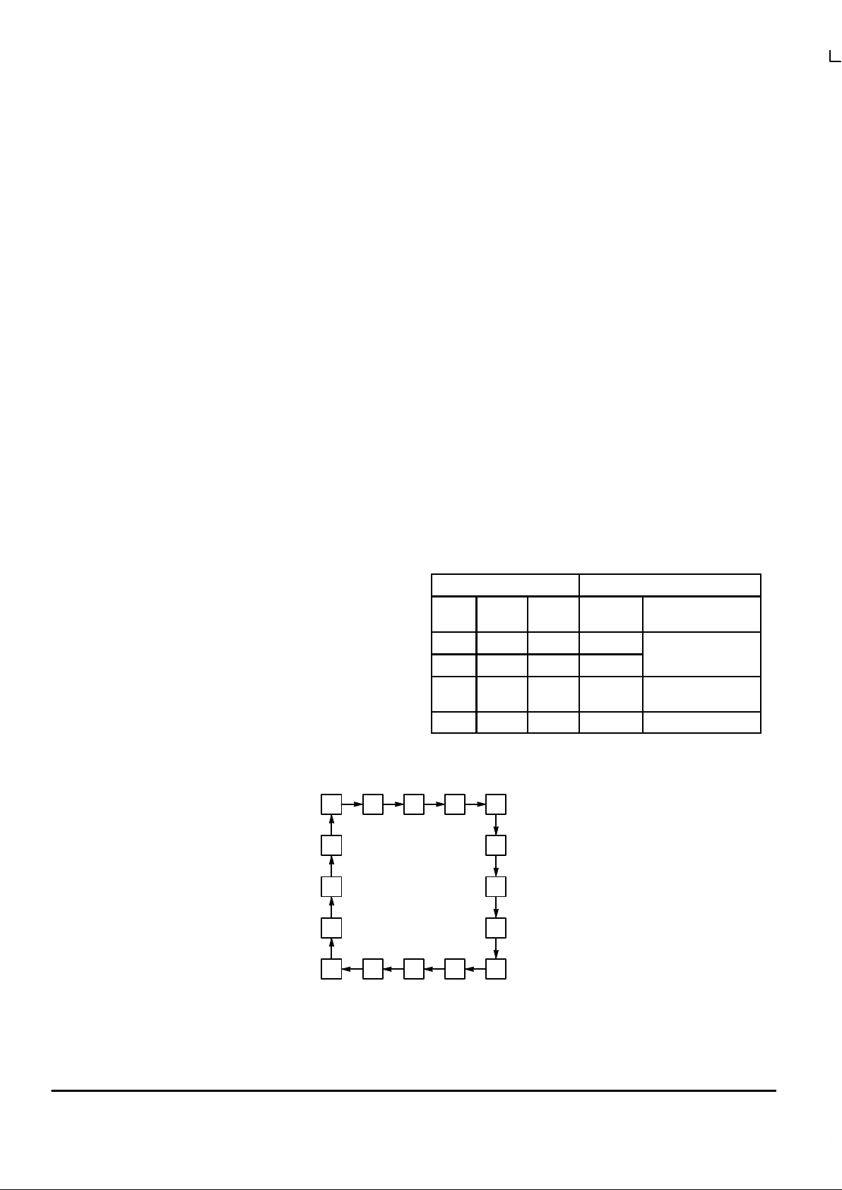
OUTPUT STATE DIAGRAM
Binary Counters
0
15
14
13
12
1 2 3 4
5
6
7
811 10 9
 Loading...