

Motorola MC74HCT157AN, MC74HCT157AD Datasheet
Î
Î
ÎÎÎ
Î
Î
Î
ÎÎÎ
Î
ÎÎÎ
ÎÎÎ
ÎÎÎ
SEMICONDUCTOR TECHNICAL DATA
$ $# #
#!$# &! %#
# $#"
High–Performance Silicon–Gate CMOS
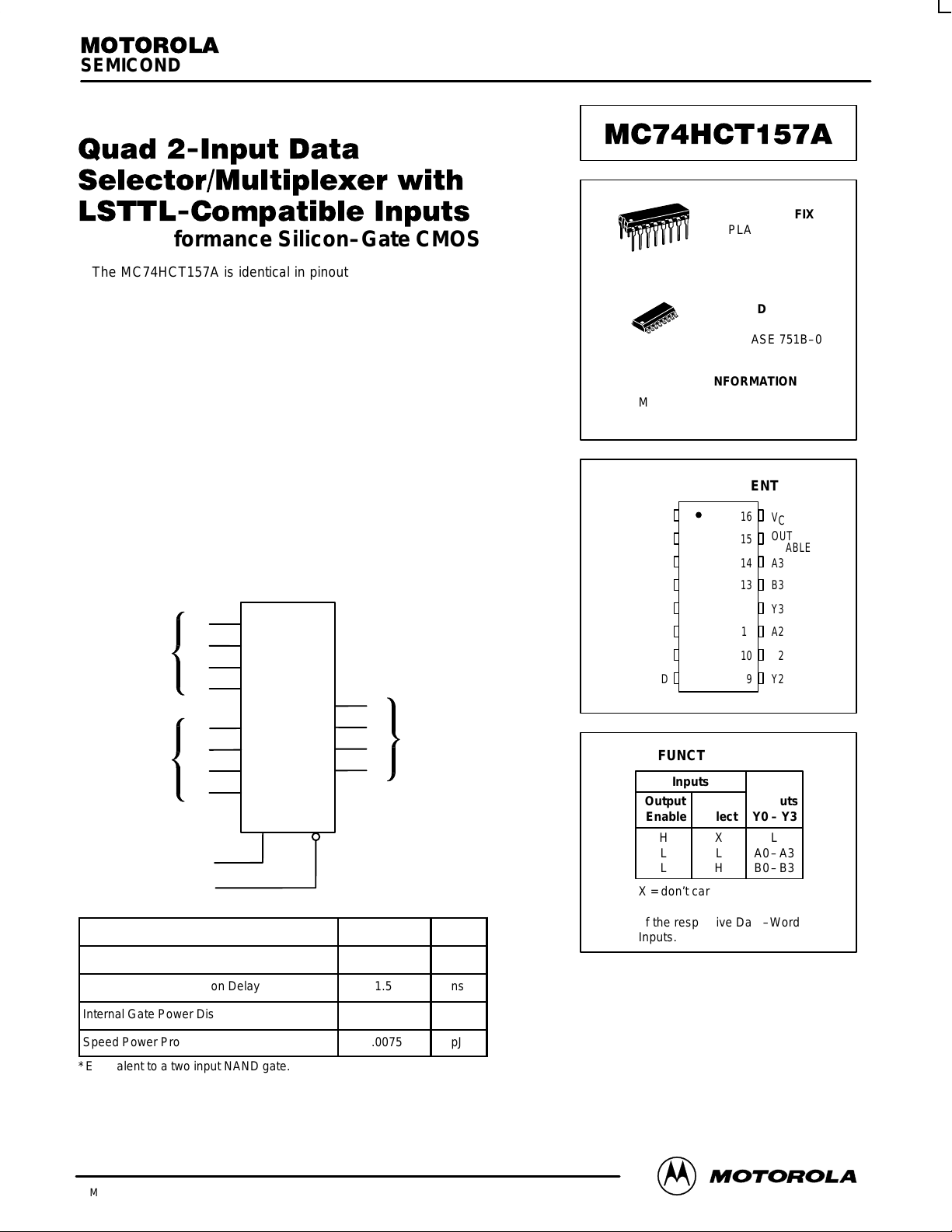
The MC74HCT157A is identical in pinout to the LS157. This device may
be used as a level converter for interfacing TTL or NMOS outputs to High
Speed CMOS inputs.
This device routes 2 nibbles (A or B) to a single port (Y) as determined by
the Select input. The data is presented at the outputs in noninverted form. A
high level on the Output Enable input sets all four Y outputs to a low level.
The HCT157A is similar in function to the HC257 which has 3–state
outputs.
• Output Drive Capability: 10 LSTTL Loads
• TTL NMOS Compatible Input Levels
• Outputs Directly Interface to CMOS, NMOS and TTL
• Operating Voltage Range: 4.5 to 5.5 V
• Low Input Current: 1.0 µA
• In Compliance with the Requirements Defined by JEDEC Standard
No. 7A
• Chip Complexity: 102 FETs or 25.5 Equivalent Gates
LOGIC DIAGRAM
2
A0
5
NIBBLE
A INPUTS
NIBBLE
B INPUTS
OUTPUT ENABLE
ОООООООООО
Internal Gate Count*
ОООООООООО
Internal Gate Propagation Delay
A1
11
A2
14
A3
3
B0
6
B1
10
B2
13
B3
SELECT
1
15
Design Criteria
4
Y0
7
Y1
9
Y2
12
Y3
PIN 16 = V
PIN 8 = GND
Value
ÎÎÎ
25.5
ÎÎÎ
1.5
DATA
OUTPUTS
CC
ÎÎ
ÎÎ
Unit
ea
ns
N SUFFIX
16
1
16
1
ORDERING INFORMATION
MC74HCTXXXAN
MC74HCTXXXAD
PIN ASSIGNMENT
SELECT
A0
B0
Y0
A1
B1
Y1
GND
FUNCTION TABLE
Inputs
Output Outputs
Enable Select Y0 – Y3
H
L
L
X = don’t care
A0 – A3, B0 – B3 = the levels
of the respective Data–Word
Inputs.
PLASTIC PACKAGE
SOIC PACKAGE
CASE 751B–05
1
2
3
4
16
15
14
13
125
6
7
11
10
8
X
L
H
CASE 648–08
D SUFFIX
Plastic
SOIC
V
CC
OUTPUT
ENABLE
A3
B3
Y3
A2
B2
Y2
9
L
A0–A3
B0–B3
Internal Gate Power Dissipation
Speed Power Product
*Equivalent to a two input NAND gate.
2/97
Motorola, Inc. 1997
1
0.005
0.0075
µW
pJ
REV 7
MC74HCT157A
Î
Î
Î
Î
Î
Î
Î
Î
Î
Î
Î
Î
Î
Î
Î
Î
Î
Î
Î
Î
Î
Î
Î
Î
Î
Î
Î
Î
Î
Î
Î
Î
Î
Î
Î
Î
Î
Î
Î
Î
Î
Î
Î
Î
Î
Î
Î
Î
Î
Î
Î
Î
Î
Î
Î
Î
Î
Î
Î
Î
Î
Î
Î
Î
Î
Î
Î
Î
Current
V
i
V
CC
GND, Other Inputs
MAXIMUM RATINGS*
Symbol
V
V
I
I
Î
T
Î
DC Supply Voltage (Referenced to GND)
CC
V
DC Input Voltage (Referenced to GND)
in
DC Output Voltage (Referenced to GND)
out
I
DC Input Current, per Pin
in
DC Output Current, per Pin
out
DC Supply Current, VCC and GND Pins
CC
P
Power Dissipation in Still Air Plastic DIP†
D
ОООООООООООО
Storage Temperature
stg
T
Lead Temperature, 1 mm from Case for 10 Seconds
L
ОООООООООООО
*Maximum Ratings are those values beyond which damage to the device may occur.
Functional operation should be restricted to the Recommended Operating Conditions.
†Derating — Plastic DIP: – 10 mW/_C from 65_ to 125_C
SOIC Package: – 7 mW/_C from 65_ to 125_C
For high frequency or heavy load considerations, see Chapter 2 of the Motorola High–Speed CMOS Data Book (DL129/D).
RECOMMENDED OPERATING CONDITIONS
Symbol
ÎÎ
V
CC
ÎÎ
Vin, V
ÎÎ
T
A
tr, t
out
f
ОООООООООООО
DC Supply Voltage (Referenced to GND)
ОООООООООООО
DC Input Voltage, Output Voltage
ОООООООООООО
(Referenced to GND)
Operating Temperature, All Package Types
Input Rise and Fall Time (Figure 1)
Parameter
SOIC Package†
(Plastic DIP or SOIC Package)
Parameter
Value
– 0.5 to + 7.0
– 0.5 to VCC + 0.5
– 0.5 to VCC + 0.5
± 20
± 25
± 50
750
500
ÎÎÎÎ
– 65 to + 150
260
ÎÎÎÎ
Min
Max
Î
Î
Î
– 55
4.5
Î
5.5
Î
0
V
CC
Î
+ 125
0
500
Unit
V
V
V
mA
mA
mA
mW
Î
_
C
_
C
Î
Unit
Î
V
Î
V
Î
_
C
ns
This device contains protection
circuitry to guard against damage
due to high static voltages or electric
fields. However, precautions must
be taken to avoid applications of any
voltage higher than maximum rated
voltages to this high–impedance circuit. For proper operation, Vin and
V
should be constrained to the
out
range GND v (Vin or V
Unused inputs must always be
tied to an appropriate logic voltage
level (e.g., either GND or VCC).
Unused outputs must be left open.
) v VCC.
out
DC ELECTRICAL CHARACTERISTICS (Voltages Referenced to GND)
Guaranteed Limit
V
Symbol
V
ÎÎ
V
ÎÎ
V
OH
ÎÎ
ÎÎÎОООООООÎООООООО
V
OL
ÎÎ
ÎÎÎОООООООÎООООООО
I
in
ÎÎ
I
CC
ÎÎ
∆I
CC
Minimum High–Level Input
IH
IL
ООООООО
Voltage
Maximum Low–Level Input
Voltage
ООООООО
Minimum High–Level Output
Voltage
ООООООО
Maximum Low–Level Output
Voltage
ООООООО
Maximum Input Leakage Current
ООООООО
Maximum Quiescent Supply
ООООООО
Current (per Package)
Additional Quiescent Supply
Parameter
Test Conditions
V
= 0.1 V or VCC – 0.1 V
out
ООООООО
|I
| v 20 µA
out
V
0.1 V or VCC – 0.1 V
out
|I
| v 20 mA
ООООООО
out
Vin = VIH or V
|I
| v 20 mA
out
ООООООО
Vin = VIH or V
|I
| v 4.0 mA
out
Vin = VIH or V
|I
| v 20 µA
ООООООО
out
Vin = VIH or V
|I
| v 4.0 mA
out
Vin = VCC or GND
ООООООО
Vin = VCC or GND
ООООООО
I
= 0 µA
out
IL
IL
IL
IL
Vin = 2.4 V, Any One Input
=
=
l
out
n
or
= 0 µA
CC
4.5
ÎÎ
5.5
4.5
5.5
ÎÎ
4.5
5.5
ÎÎ
ÎÎ
4.5
4.5
5.5
ÎÎ
4.5
ÎÎ
5.5
ÎÎ
5.5
ÎÎ
5.5
NOTE:Information on typical parametric values can be found in Chapter 2 of the Motorola High–Speed CMOS Data Book (DL129/D).
– 55 to
V
25_C
2.0
ÎÎ
2.0
0.8
0.8
ÎÎ
4 4
5.4
ÎÎ
ÎÎ
3.98
0.1
0.1
ÎÎ
0.26
ÎÎ
± 0.1
ÎÎ
4.0
ÎÎ
≥ – 55_C
2.9
v
85_Cv 125_C
2.0
ÎÎ
2.0
0.8
0.8
ÎÎ
4.4
5.4
ÎÎ
ÎÎ
3.84
0.1
0.1
ÎÎ
0.33
ÎÎ
± 1.0
ÎÎ
40
ÎÎ
25_C to 125_C
2.4
2.0
ÎÎ
2.0
0.8
0.8
ÎÎ
4.4
5.4
ÎÎ
ÎÎ
3.7
0.1
0.1
ÎÎ
0.4
ÎÎ
± 1.0
ÎÎ
160
ÎÎ
Unit
Î
Î
Î
Î
Î
Î
µA
Î
µA
Î
mA
V
V
V
V
MOTOROLA High–Speed CMOS Logic Data
2
DL129 — Rev 6
 Loading...