

MOTOROLA MC74HC374ADTEL, MC74HC374ADTR2, MC74HC374ADT, MC74HC374AFR1, MC74HC374AFR2 Datasheet
...
Semiconductor Components Industries, LLC, 2000
March, 2000 – Rev. 8
1 Publication Order Number:
MC74HC374A/D
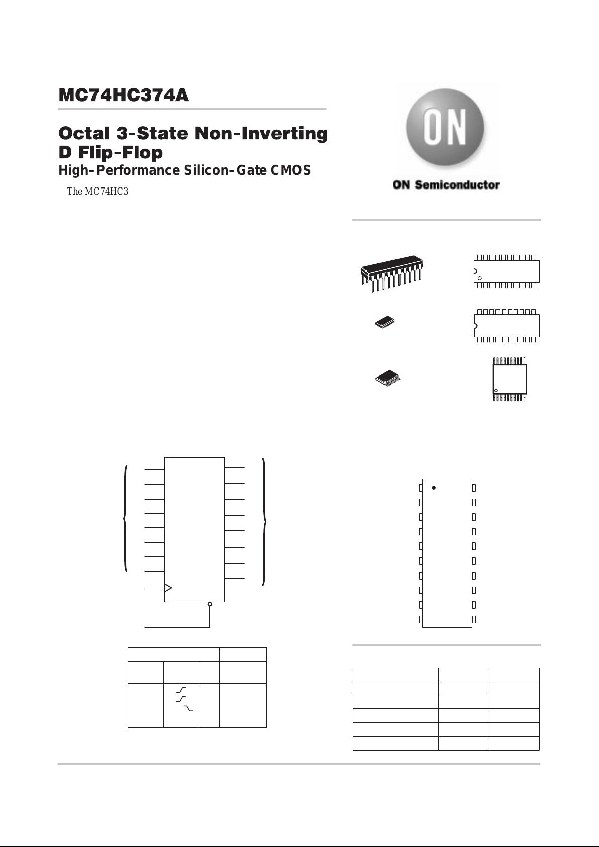
MC74HC374A
Octal 3-State Non-Inverting
D Flip-Flop
High–Performance Silicon–Gate CMOS
The MC74HC374A is identical in pinout to the LS374. The device
inputs are compatible with standard CMOS outputs; with pullup
resistors, they are compatible with LSTTL outputs.
Data meeting the setup time is clocked to the outputs with the rising
edge of the clock. The Output Enable input does not affect the states of
the flip–flops, but when Output Enable is high, the outputs are forced
to the high–impedance state; thus, data may be stored even when the
outputs are not enabled.
The HC374A is identical in function to the HC574A which has the
input pins on the opposite side of the package from the output. This
device is similar in function to the HC534A which has inverting
outputs.
• Output Drive Capability: 15 LSTTL Loads
• Outputs Directly Interface to CMOS, NMOS, and TTL
• Operating Voltage Range: 2.0 to 6.0 V
• Low Input Current: 1.0 µA
• High Noise Immunity Characteristic of CMOS Devices
• In Compliance with the Requirements Defined by JEDEC Standard
No. 7A
• Chip Complexity: 266 FETs or 66.5 Equivalent Gates
LOGIC DIAGRAM
DATA
INPUTS
D0
11
CLOCK
D1
D2
D3
D4
D5
D6
D7
18
17
14
13
8
7
4
3
1
OUTPUT ENABLE
19
Q0
Q1
Q2
Q3
Q4
Q5
Q6
Q7
16
15
12
9
6
5
2
PIN 20 = V
CC
PIN 10 = GND
NONINVERTING
OUTPUTS
FUNCTION TABLE
Inputs Output
Output
Enable Clock D Q
LHH
LLL
L L,H, X No Change
HXXZ
X = don’t care
Z = high impedance
http://onsemi.com
MARKING
DIAGRAMS
1
20
A = Assembly Location
WL = Wafer Lot
YY = Year
WW = Work Week
SOIC WIDE–20
DW SUFFIX
CASE 751D
HC374A
AWLYYWW
PDIP–20
N SUFFIX
CASE 738
1
20
MC74HC374AN
AWLYYWW
TSSOP–20
DT SUFFIX
CASE 948G
1
20
1
20
1
20
Device Package Shipping
ORDERING INFORMATION
MC74HC374AN PDIP–20 1440 / Box
MC74HC374ADW SOIC–WIDE
38 / Rail
MC74HC374ADWR2 SOIC–WIDE 1000 / Reel
MC74HC374ADT TSSOP–20 75 / Rail
MC74HC374ADTR2 TSSOP–20
2500 / Reel
HC
374A
ALYW
1
20
PIN ASSIGNMENT
Q2
D1
D0
Q0
OUTPUT
ENABLE
GND
Q3
D3
D2
Q1 5
4
3
2
1
10
9
8
7
6
14
15
16
17
18
19
20
11
12
13
Q6
D6
D7
Q7
V
CC
CLOCK
Q4
D4
D5
Q5
MC74HC374A
http://onsemi.com
2
MAXIMUM RATINGS*
Symbol
Parameter
Value
Unit
V
CC
DC Supply Voltage (Referenced to GND)
– 0.5 to + 7.0
V
V
in
DC Input Voltage (Referenced to GND)
– 0.5 to VCC + 0.5
V
V
out
DC Output Voltage (Referenced to GND)
– 0.5 to VCC + 0.5
V
I
in
DC Input Current, per Pin
± 20
mA
I
out
DC Output Current, per Pin
± 35
mA
I
CC
DC Supply Current, VCC and GND Pins
± 75
mA
ÎÎ
Î
P
D
ОООООООООООО
Î
Power Dissipation in Still Air, Plastic DIP†
SOIC Package†
TSSOP Package†
ÎÎÎ
Î
750
500
450
Î
Î
mW
T
stg
Storage Temperature
– 65 to + 150
_
C
ÎÎ
Î
T
L
ОООООООООООО
Î
Lead Temperature, 1 mm from Case for 10 Seconds
(Plastic DIP, SOIC, SSOP or TSSOP Package)
ÎÎÎ
Î
260
Î
Î
_
C
*Maximum Ratings are those values beyond which damage to the device may occur.
Functional operation should be restricted to the Recommended Operating Conditions.
†Derating — Plastic DIP: – 10 mW/_C from 65_ to 125_C
SOIC Package: – 7 mW/_C from 65_ to 125_C
TSSOP Package: – 6.1 mW/_C from 65_ to 125_C
For high frequency or heavy load considerations, see Chapter 2 of the ON Semiconductor High–Speed CMOS Data Book (DL129/D).
RECOMMENDED OPERATING CONDITIONS
Symbol
Parameter
Min
ÎÎ
Max
Unit
V
CC
DC Supply Voltage (Referenced to GND)
2.0
ÎÎ
6.0
V
Vin, V
out
DC Input Voltage, Output Voltage (Referenced to GND)
0
ÎÎ
V
CC
V
T
A
Operating Temperature, All Package Types
– 55
ÎÎ
+ 125
_
C
ÎÎ
Î
tr, t
f
ООООООООООООО
Î
Input Rise and Fall Time VCC = 2.0 V
(Figure 1) VCC = 4.5 V
VCC = 6.0 V
Î
Î
0
0
0
ÎÎ
ÎÎ
1000
500
400
Î
Î
ns
DC ELECTRICAL CHARACTERISTICS (Voltages Referenced to GND)
Guaranteed Limit
ÎÎ
Î
Symbol
ООООООО
Î
Parameter
ООООООО
Î
Test Conditions
ÎÎ
Î
V
CC
V
ÎÎ
Î
– 55 to
25_C
ÎÎÎ
Î
Î
Î
v
85_C
ÎÎ
Î
v
125_C
Î
Î
Unit
ÎÎ
Î
ÎÎ
Î
V
IH
ООООООО
Î
ООООООО
Î
Minimum High–Level Input
Voltage
ООООООО
Î
ООООООО
Î
V
out
= 0.1 V or VCC – 0.1 V
|I
out
| v 20 µA
ÎÎ
Î
ÎÎ
Î
2.0
3.0
4.5
6.0
ÎÎ
Î
ÎÎ
Î
1.50
2.10
3.15
4.20
ÎÎÎ
Î
Î
Î
Î
Î
Î
1.50
2.10
3.15
4.20
ÎÎ
Î
ÎÎ
Î
1.50
2.10
3.15
4.20
Î
Î
Î
Î
V
ÎÎ
Î
ÎÎ
Î
V
IL
ООООООО
Î
ООООООО
Î
Maximum Low–Level Input
Voltage
ООООООО
Î
ООООООО
Î
V
out
= 0.1 V or VCC – 0.1 V
|I
out
| v 20 µA
ÎÎ
Î
ÎÎ
Î
2.0
3.0
4.5
6.0
ÎÎ
Î
ÎÎ
Î
0.50
0.90
1.35
1.80
ÎÎÎ
Î
Î
Î
Î
Î
Î
0.50
0.90
1.35
1.80
ÎÎ
Î
ÎÎ
Î
0.50
0.90
1.35
1.80
Î
Î
Î
Î
V
ÎÎ
Î
V
OH
ООООООО
Î
Minimum High–Level Output
Voltage
ООООООО
Î
Vin = VIH or V
IL
|I
out
| v 20 µA
ÎÎ
Î
2.0
4.5
6.0
ÎÎ
Î
1.90
4.40
5.90
ÎÎÎ
Î
Î
Î
1.90
4.40
5.90
ÎÎ
Î
1.90
4.40
5.90
Î
Î
V
ÎÎ
Î
ÎÎ
Î
ООООООО
Î
ООООООО
Î
ООООООО
Î
ООООООО
Î
Vin = VIH or VIL|I
out
| v 2.4 mA
|I
out
| v 6.0 mA
|I
out
| v 7.8 mA
ÎÎ
Î
ÎÎ
Î
3.0
4.5
6.0
ÎÎ
Î
ÎÎ
Î
2.48
2.98
5.48
ÎÎÎ
Î
Î
Î
Î
Î
Î
2.34
3.84
5.34
ÎÎ
Î
ÎÎ
Î
2.20
3.70
5.20
Î
Î
Î
Î
V
This device contains protection
circuitry to guard against damage
due to high static voltages or electric
fields. However, precautions must
be taken to avoid applications of any
voltage higher than maximum rated
voltages to this high–impedance circuit. For proper operation, Vin and
V
out
should be constrained to the
range GND v (Vin or V
out
) v VCC.
Unused inputs must always be
tied to an appropriate logic voltage
level (e.g., either GND or VCC).
Unused outputs must be left open.
MC74HC374A
http://onsemi.com
3
DC ELECTRICAL CHARACTERISTICS (Voltages Referenced to GND)
Unit
Guaranteed Limit
V
CC
V
Test Conditions
Parameter
Symbol
Unit
v
125_C
ÎÎÎ
v
85_C
– 55 to
25_C
V
CC
V
Test Conditions
Parameter
Symbol
ÎÎ
Î
ÎÎ
Î
V
OL
ООООООО
Î
ООООООО
Î
Maximum Low–Level Output
Voltage
ООООООО
Î
ООООООО
Î
Vin = VIH or V
IL
|I
out
| v 20 µA
ÎÎ
Î
ÎÎ
Î
2.0
4.5
6.0
ÎÎ
Î
ÎÎ
Î
0.10
0.10
0.10
ÎÎÎ
Î
Î
Î
Î
Î
Î
0.10
0.10
0.10
ÎÎ
Î
ÎÎ
Î
0.10
0.10
0.10
Î
Î
Î
Î
V
ÎÎÎОООООООÎООООООО
Î
Vin = VIH or VIL|I
out
| v 2.4 mA
|I
out
| v 6.0 mA
|I
out
| v 7.8 mA
ÎÎ
Î
3.0
4.5
6.0
ÎÎ
Î
0.26
0.26
0.26
ÎÎÎ
Î
Î
Î
0.33
0.33
0.33
ÎÎ
Î
0.40
0.40
0.40
Î
Î
V
ÎÎ
Î
I
in
ООООООО
Î
Maximum Input Leakage
Current
ООООООО
Î
Vin = VCC or GND
ÎÎ
Î
6.0
ÎÎ
Î
± 0.1
ÎÎÎ
Î
Î
Î
± 1.0
ÎÎ
Î
± 1.0
Î
Î
µA
ÎÎ
Î
I
OZ
ООООООО
Î
Maximum Three–State
Leakage Current
ООООООО
Î
Output in High–Impedance State
Vin = VIL or V
IH
V
out
= VCC or GND
ÎÎ
Î
6.0
ÎÎ
Î
± 0.5
ÎÎÎ
Î
Î
Î
± 5.0
ÎÎ
Î
± 10
Î
Î
µA
ÎÎ
Î
I
CC
ООООООО
Î
Maximum Quiescent Supply
Current (per Package)
ООООООО
Î
Vin = VCC or GND
I
out
= 0 µA
ÎÎ
Î
6.0
ÎÎ
Î
4
ÎÎÎ
Î
Î
Î
40
ÎÎ
Î
160
Î
Î
µA
NOTE: Information on typical parametric values can be found in Chapter 2 of the ON Semiconductor High–Speed CMOS Data Book
(DL129/D).
AC ELECTRICAL CHARACTERISTICS (C
L
= 50 pF, Input tr = tf = 6.0 ns)
Guaranteed Limit
ÎÎÎ
Î
Symbol
ОООООООООООООО
Î
Parameter
ÎÎ
Î
V
CC
V
ÎÎ
Î
– 55 to
25_C
ÎÎÎ
Î
Î
Î
v
85_C
ÎÎ
Î
v
125_C
Î
Î
Unit
ÎÎÎ
Î
ÎÎÎ
Î
f
max
ОООООООООООООО
Î
ОООООООООООООО
Î
Maximum Clock Frequency (50% Duty Cycle)
ÎÎ
Î
ÎÎ
Î
2.0
3.0
4.5
6.0
ÎÎ
Î
ÎÎ
Î
6
15
30
35
ÎÎÎ
Î
Î
Î
Î
Î
Î
5
10
24
28
ÎÎ
Î
ÎÎ
Î
4
8
20
24
Î
Î
Î
Î
MHz
ÎÎÎ
Î
t
PLH
t
PHL
ОООООООООООООО
Î
Maximum Propagation Delay, Input Clock to Q
(Figures 1 and 5)
ÎÎ
Î
2.0
3.0
4.5
6.0
ÎÎ
Î
125
80
25
21
ÎÎÎ
Î
Î
Î
155
110
31
26
ÎÎ
Î
190
130
38
32
Î
Î
ns
ÎÎÎ
Î
ÎÎÎ
Î
t
PLZ
t
PHZ
ОООООООООООООО
Î
ОООООООООООООО
Î
Maximum Propagation Delay, Output Enable to Q
(Figures 3 and 6)
ÎÎ
Î
ÎÎ
Î
2.0
3.0
4.5
6.0
ÎÎ
Î
ÎÎ
Î
150
100
30
26
ÎÎÎ
Î
Î
Î
Î
Î
Î
190
125
38
33
ÎÎ
Î
ÎÎ
Î
225
150
45
38
Î
Î
Î
Î
ns
ÎÎÎ
Î
ÎÎÎ
Î
t
PLZ
t
PHZ
ОООООООООООООО
Î
ОООООООООООООО
Î
Maximum Propagation Delay, Output Enable to Q
(Figures 3 and 6)
ÎÎ
Î
ÎÎ
Î
2.0
3.0
4.5
6.0
ÎÎ
Î
ÎÎ
Î
150
100
30
26
ÎÎÎ
Î
Î
Î
Î
Î
Î
190
125
38
33
ÎÎ
Î
ÎÎ
Î
225
150
45
38
Î
Î
Î
Î
ns
ÎÎÎ
Î
ÎÎÎ
Î
t
TLH
t
THL
ОООООООООООООО
Î
ОООООООООООООО
Î
Maximum Output Transition Time, Any Output
(Figures 1 and 5)
ÎÎ
Î
ÎÎ
Î
2.0
3.0
4.5
6.0
ÎÎ
Î
ÎÎ
Î
75
27
15
13
ÎÎÎ
Î
Î
Î
Î
Î
Î
95
32
19
16
ÎÎ
Î
ÎÎ
Î
110
36
22
19
Î
Î
Î
Î
ns
C
in
Maximum Input Capacitance
10
ÎÎÎ
10
10
pF
ÎÎÎ
Î
C
out
ОООООООООООООО
Î
Maximum Three–State Output Capacitance
(Output in High–Impedance State)
ÎÎÎÎÎ
Î
15
ÎÎÎ
Î
Î
Î
15
ÎÎ
Î
15
Î
Î
pF
NOTE: For propagation delays with loads other than 50 pF, and information on typical parametric values, see Chapter 2 of the ON
Semiconductor High–Speed CMOS Data Book (DL129/D).
Typical @ 25°C, VCC = 5.0 V
C
PD
Power Dissipation Capacitance (Per Enabled Output)*
34
pF
*Used to determine the no–load dynamic power consumption: PD = CPD V
CC
2
f + ICC VCC. For load considerations, see Chapter 2 of the
ON Semiconductor High–Speed CMOS Data Book (DL129/D).
 Loading...