

MOTOROLA MC74HC132AN, MC74HC132AFL1, MC74HC132AFL2, MC74HC132AFR1, MC74HC132AFR2 Datasheet
...
Semiconductor Components Industries, LLC, 2000
March, 2000 – Rev. 7
1 Publication Order Number:
MC74HC132A/D
MC74HC132A
Quad 2-Input NAND Gate
with Schmitt-Trigger Inputs
High–Performance Silicon–Gate CMOS
The MC74HC132A is identical in pinout to the LS132. The device
inputs are compatible with standard CMOS outputs; with pullup
resistors, they are compatible with LSTTL outputs.
The HC132A can be used to enhance noise immunity or to square up
slowly changing waveforms.
• Output Drive Capability: 10 LSTTL Loads
• Outputs Directly Interface to CMOS, NMOS, and TTL
• Operating Voltage Range: 2.0 to 6.0 V
• Low Input Current: 1.0 µA
• High Noise Immunity Characteristic of CMOS Devices
• In Compliance with the Requirements Defined by JEDEC Standard
No. 7A
• Chip Complexity: 72 FETs or 18 Equivalent Gates
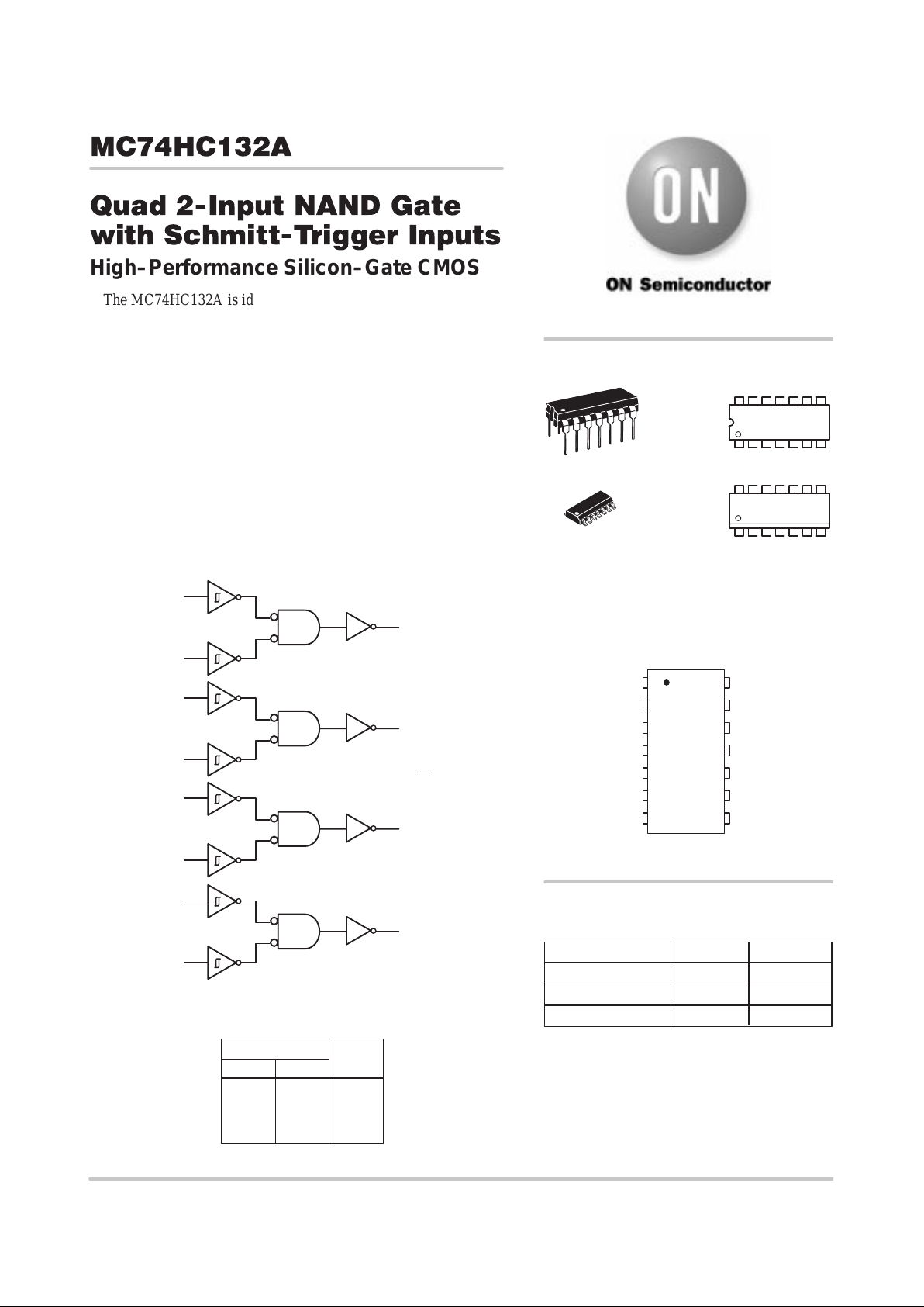
LOGIC DIAGRAM
A1
B1
Y1
3
2
1
PIN 14 = V
CC
PIN 7 = GND
Y = AB
A2
B2
Y2
6
5
4
A3
B3
Y3
8
10
9
A4
B4
Y4
11
13
12
FUNCTION TABLE
Inputs Output
ABY
LLH
LHH
HLH
HHL
Device Package Shipping
ORDERING INFORMATION
MC74HC132AN PDIP–14 2000 / Box
MC74HC132AD SOIC–14
http://onsemi.com
55 / Rail
MC74HC132ADR2 SOIC–14 2500 / Reel
MARKING
DIAGRAMS
A = Assembly Location
WL or L = Wafer Lot
YY or Y = Year
WW or W = Work Week
1
14
PDIP–14
N SUFFIX
CASE 646
MC74HC132AN
AWLYYWW
SOIC–14
D SUFFIX
CASE 751A
1
14
HC132A
AWLYWW
PIN ASSIGNMENT
11
12
13
14
8
9
105
4
3
2
1
7
6
B3
Y4
A4
B4
V
CC
Y3
A3
A2
Y1
B1
A1
GND
Y2
B2
MC74HC132A
http://onsemi.com
2
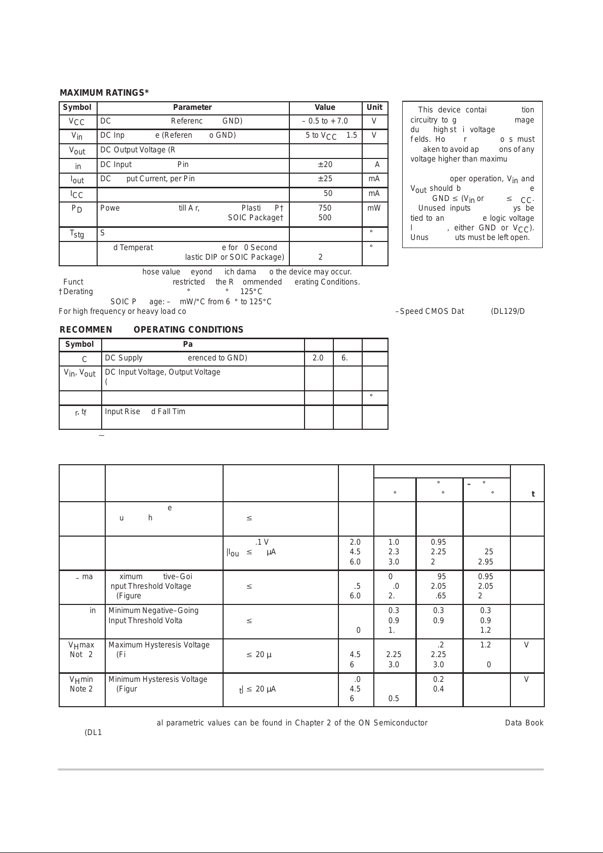
MAXIMUM RATINGS*
Symbol
Parameter
Value
Unit
V
CC
DC Supply Voltage (Referenced to GND)
– 0.5 to + 7.0
V
V
in
DC Input Voltage (Referenced to GND)
– 1.5 to VCC + 1.5
V
V
out
DC Output Voltage (Referenced to GND)
– 0.5 to VCC + 0.5
V
I
in
DC Input Current, per Pin
± 20
mA
I
out
DC Output Current, per Pin
± 25
mA
I
CC
DC Supply Current, VCC and GND Pins
± 50
mA
ÎÎ
Î
P
D
ОООООООООООО
Î
Power Dissipation in Still Air, Plastic DIP†
SOIC Package†
ÎÎÎ
Î
750
500
Î
Î
mW
T
stg
Storage Temperature
– 65 to + 150
_
C
ÎÎ
Î
T
L
ОООООООООООО
Î
Lead Temperature, 1 mm from Case for 10 Seconds
(Plastic DIP or SOIC Package)
ÎÎÎ
Î
260
Î
Î
_
C
*Maximum Ratings are those values beyond which damage to the device may occur.
Functional operation should be restricted to the Recommended Operating Conditions.
†Derating — Plastic DIP: – 10 mW/_C from 65_ to 125_C
SOIC Package: – 7 mW/_C from 65_ to 125_C
For high frequency or heavy load considerations, see Chapter 2 of the ON Semiconductor High–Speed CMOS Data Book (DL129/D).
RECOMMENDED OPERATING CONDITIONS
Symbol
Parameter
Min
ÎÎ
Max
Unit
V
CC
DC Supply Voltage (Referenced to GND)
2.0
ÎÎ
6.0
V
ÎÎ
Î
Vin, V
out
ООООООООООООО
Î
DC Input Voltage, Output Voltage
(Referenced to GND)
Î
Î
0
ÎÎ
ÎÎ
V
CC
Î
Î
V
T
A
Operating Temperature, All Package Types
– 55
ÎÎ
+ 125
_
C
ÎÎ
Î
tr, t
f
ООООООООООООО
Î
Input Rise and Fall Time (Figure 1)
Î
Î
—
ÎÎ
ÎÎ
no
limit*
Î
Î
ns
*When Vin X 0.5 VCC, ICC >> quiescent current.
DC ELECTRICAL CHARACTERISTICS (Voltages Referenced to GND)
Guaranteed Limit
Symbol
Parameter
Test Conditions
V
CC
V
25_C
– 40_C to
+ 85_C
– 55_C to
+ 125_C
Unit
ÎÎ
Î
ÎÎ
Î
VT+ max
ООООООО
Î
ООООООО
Î
Maximum Positive–Going
Input Threshold Voltage
(Figure 3)
ООООООО
Î
ООООООО
Î
V
out
= 0.1 V
|I
out
| v 20 µA
Î
Î
Î
Î
2.0
4.5
6.0
ÎÎ
Î
ÎÎ
Î
1.5
3.15
4.2
ÎÎ
Î
ÎÎ
Î
1.5
3.15
4.2
ÎÎ
Î
ÎÎ
Î
1.5
3.15
4.2
Î
Î
Î
Î
V
ÎÎ
Î
VT+ min
ООООООО
Î
Minimum Positive–Going
Input Threshold Voltage
(Figure 3)
ООООООО
Î
V
out
= 0.1 V
|I
out
| v 20 µA
Î
Î
2.0
4.5
6.0
ÎÎ
Î
1.0
2.3
3.0
ÎÎ
Î
0.95
2.25
2.95
ÎÎ
Î
0.95
2.25
2.95
Î
Î
V
ÎÎ
Î
VT– max
ООООООО
Î
Maximum Negative–Going
Input Threshold Voltage
(Figure 3)
ООООООО
Î
V
out
= VCC – 0.1 V
|I
out
| v 20 µA
Î
Î
2.0
4.5
6.0
ÎÎ
Î
0.9
2.0
2.6
ÎÎ
Î
0.95
2.05
2.65
ÎÎ
Î
0.95
2.05
2.65
Î
Î
V
ÎÎ
Î
VT– min
ООООООО
Î
Minimum Negative–Going
Input Threshold Voltage
(Figure 3)
ООООООО
Î
V
out
= VCC – 0.1 V
|I
out
| v 20 µA
Î
Î
2.0
4.5
6.0
ÎÎ
Î
0.3
0.9
1.2
ÎÎ
Î
0.3
0.9
1.2
ÎÎ
Î
0.3
0.9
1.2
Î
Î
V
ÎÎ
Î
ÎÎ
Î
VHmax
Note 2
ООООООО
Î
ООООООО
Î
Maximum Hysteresis Voltage
(Figure 3)
ООООООО
Î
ООООООО
Î
V
out
= 0.1 V or VCC – 0.1 V
|I
out
| v 20 µA
Î
Î
Î
Î
2.0
4.5
6.0
ÎÎ
Î
ÎÎ
Î
1.2
2.25
3.0
ÎÎ
Î
ÎÎ
Î
1.2
2.25
3.0
ÎÎ
Î
ÎÎ
Î
1.2
2.25
3.0
Î
Î
Î
Î
V
ÎÎ
Î
VHmin
Note 2
ООООООО
Î
Minimum Hysteresis Voltage
(Figure 3)
ООООООО
Î
V
out
= 0.1 V or VCC – 0.1 V
|I
out
| v 20 µA
Î
Î
2.0
4.5
6.0
ÎÎ
Î
0.2
0.4
0.5
ÎÎ
Î
0.2
0.4
0.5
ÎÎ
Î
0.2
0.4
0.5
Î
Î
V
NOTE: 1. VHmin > (VT+ min) – (VT– max); VHmax = (VT+ max) + (VT– min).
NOTE: Information on typical parametric values can be found in Chapter 2 of the ON Semiconductor High–Speed CMOS Data Book
(DL129/D).
This device contains protection
circuitry to guard against damage
due to high static voltages or electric
fields. However, precautions must
be taken to avoid applications of any
voltage higher than maximum rated
voltages to this high–impedance circuit. For proper operation, Vin and
V
out
should be constrained to the
range GND v (Vin or V
out
) v VCC.
Unused inputs must always be
tied to an appropriate logic voltage
level (e.g., either GND or VCC).
Unused outputs must be left open.
MC74HC132A
http://onsemi.com
3
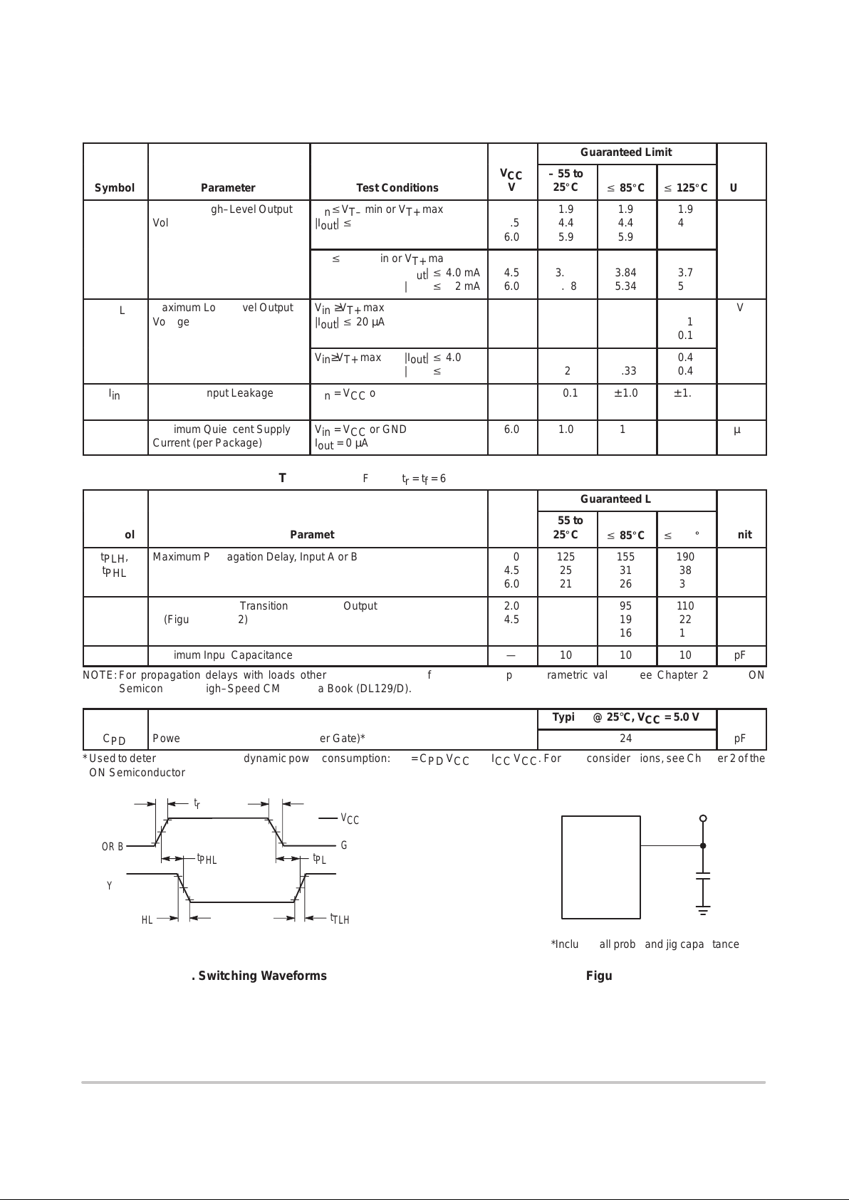
DC ELECTRICAL CHARACTERISTICS (Voltages Referenced to GND)
Guaranteed Limit
ÎÎ
Î
Symbol
ООООООО
Î
Parameter
ООООООО
Î
Test Conditions
ÎÎ
Î
V
CC
V
ÎÎ
Î
– 55 to
25_C
ÎÎÎ
Î
Î
Î
v
85_C
ÎÎ
Î
v
125_C
Î
Î
Unit
ÎÎ
Î
V
OH
ООООООО
Î
Minimum High–Level Output
Voltage
ООООООО
Î
Vinv
VT– min or VT+ max
|I
out
| v 20 µA
ÎÎ
Î
2.0
4.5
6.0
ÎÎ
Î
1.9
4.4
5.9
ÎÎÎ
Î
Î
Î
1.9
4.4
5.9
ÎÎ
Î
1.9
4.4
5.9
Î
Î
V
ÎÎÎОООООООÎООООООО
Î
Vinv
–VT– min or VT+ max
|I
out
| v 4.0 mA
|I
out
| v 5.2 mA
ÎÎ
Î
4.5
6.0
ÎÎ
Î
3.98
5.48
ÎÎÎ
Î
Î
Î
3.84
5.34
ÎÎ
Î
3.7
5.2
Î
Î
ÎÎ
Î
V
OL
ООООООО
Î
Maximum Low–Level Output
Voltage
ООООООО
Î
Vin ≥VT+ max
|I
out
| v 20 µA
ÎÎ
Î
2.0
4.5
6.0
ÎÎ
Î
0.1
0.1
0.1
ÎÎÎ
Î
Î
Î
0.1
0.1
0.1
ÎÎ
Î
0.1
0.1
0.1
Î
Î
V
ÎÎÎОООООООÎООООООО
Î
Vin≥VT+ max |I
out
| v 4.0 mA
|I
out
| v 5.2 mA
ÎÎ
Î
4.5
6.0
ÎÎ
Î
0.26
0.26
ÎÎÎ
Î
Î
Î
0.33
0.33
ÎÎ
Î
0.4
0.4
Î
Î
ÎÎ
Î
I
in
ООООООО
Î
Maximum Input Leakage
Current
ООООООО
Î
Vin = VCC or GND
ÎÎ
Î
6.0
ÎÎ
Î
± 0.1
ÎÎÎ
Î
Î
Î
± 1.0
ÎÎ
Î
± 1.0
Î
Î
µA
ÎÎ
Î
I
CC
ООООООО
Î
Maximum Quiescent Supply
Current (per Package)
ООООООО
Î
Vin = VCC or GND
I
out
= 0 µA
ÎÎ
Î
6.0
ÎÎ
Î
1.0
ÎÎÎ
Î
Î
Î
10
ÎÎ
Î
40
Î
Î
µA
AC ELECTRICAL CHARACTERISTICS (C
L
= 50 pF, Input tr = tf = 6.0 ns)
Guaranteed Limit
ÎÎ
Î
Symbol
ООООООООООООООО
Î
Parameter
ÎÎ
Î
V
CC
V
ÎÎ
Î
– 55 to
25_C
ÎÎÎ
Î
Î
Î
v
85_C
ÎÎ
Î
v
125_C
Î
Î
Unit
ÎÎ
Î
t
PLH
,
t
PHL
ООООООООООООООО
Î
Maximum Propagation Delay, Input A or B to Output Y
(Figures 1 and 2)
ÎÎ
Î
2.0
4.5
6.0
ÎÎ
Î
125
25
21
ÎÎÎ
Î
Î
Î
155
31
26
ÎÎ
Î
190
38
32
Î
Î
ns
ÎÎ
Î
t
TLH
,
t
THL
ООООООООООООООО
Î
Maximum Output Transition Time, Any Output
(Figures 1 and 2)
ÎÎ
Î
2.0
4.5
6.0
ÎÎ
Î
75
15
13
ÎÎÎ
Î
Î
Î
95
19
16
ÎÎ
Î
110
22
19
Î
Î
ns
C
in
Maximum Input Capacitance
—
10
ÎÎÎ
10
10
pF
NOTE: For propagation delays with loads other than 50 pF, and information on typical parametric values, see Chapter 2 of the ON
Semiconductor High–Speed CMOS Data Book (DL129/D).
Typical @ 25°C, VCC = 5.0 V
C
PD
Power Dissipation Capacitance (Per Gate)*
24
pF
*Used to determine the no–load dynamic power consumption: PD = CPD V
CC
2
f + ICC VCC. For load considerations, see Chapter 2 of the
ON Semiconductor High–Speed CMOS Data Book (DL129/D).
Figure 1. Switching Waveforms
t
r
V
CC
GND
90%
50%
10%
90%
50%
10%
INPUT
A OR B
Y
t
PHL
t
PLH
t
THL
t
TLH
*Includes all probe and jig capacitance
Figure 2. Test Circuit
CL*
TEST POINT
DEVICE
UNDER
TEST
OUTPUT
t
f
 Loading...