

Motorola MC74F779N, MC74F779J, MC74F779D Datasheet
4-252
FAST AND LS TTL DATA
8-BIT BIDIRECTIONAL
BINARY COUNTER (3-STATE)
The MC74F779 is a fully synchronous 8-stage up/down counter with multiplexed 3-state I/O ports for bus-oriented applications. All control functions
(hold, count up, count down, synchronous load) are controlled by two mode
pins (S0, S1). The device also features carry look-ahead for easy cascading.
All state changes are initiated by the rising edge of the clock.
When CET
is High the data outputs are held in their current state and TC
is held high. The TC output is not recommended for use as a clock or asynchronous reset due to the possibility of decoding spikes.
• Multiplexed 3-State I/O Ports For Bus-oriented Applications
• Built-In Look-Ahead Carry Capability
• Count Frequency 145 MHz Typ
• Supply Current 90 mA Typ
• Fully Synchronous Operation
• Separate Pins for Master Reset and Synchronous Reset
• Center Power Pins to Reduce Effects of Package Inductance
• See F269 for 24-Pin Separate I/O Port Version
• See F579 for 20-Pin Version
• ESD Protection > 4000 Volts
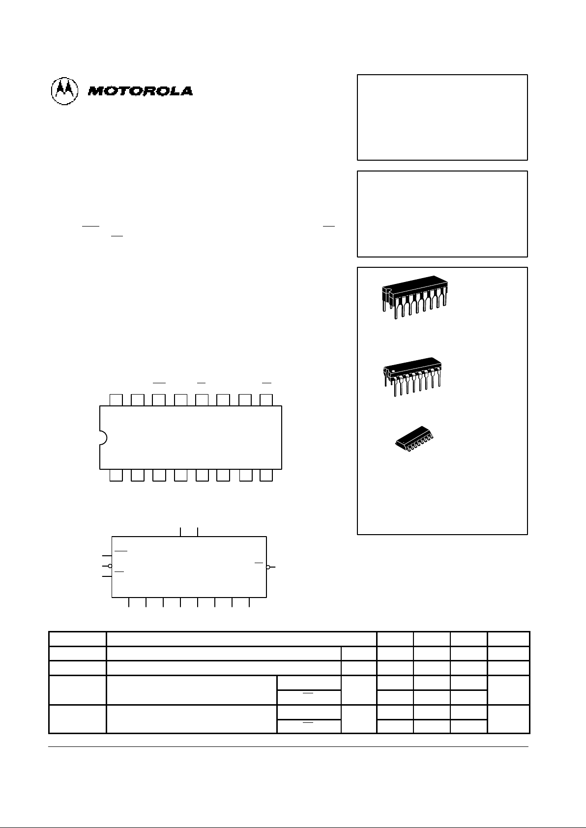
14 13 12 11 10 9
1 2 3 4 5 6
7
16 15
8
I/O
0
I/O
1
CP CET VCCTC S
1
S
0
OE
I/O2I/O3GND I/O4I/O5I/O6I/O
7
PIN ASSIGNMENT
LOGIC SYMBOL
TC
I/O0I/O1I/O2I/O3I/O4I/O5I/O6I/O
7
2 3 4 5 6 7 8 9
12
CP
OE
CET
15
9
14
S0S
1
11 10
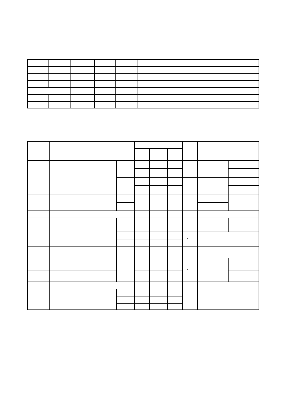
GUARANTEED OPERATING RANGES
Symbol Parameter Min Typ Max Unit
V
CC
Supply Voltage 74 4.5 5.0 5.5 V
T
A
Operating Ambient Temperature Range 74 0 25 70 °C
I/O0–I/O
7
–3.0
IOHOutput Current — High
TC
74
–1.0
mA
I/O0–I/O
7
24
IOLOutput Current — Low
TC
7420mA
MC74F779
8-BIT BIDIRECTIONAL
BINARY COUNTER (3-STATE)
J SUFFIX
CERAMIC
CASE 620-09
N SUFFIX
PLASTIC
CASE 648-08
16
1
16
1
ORDERING INFORMATION
MC74FXXXJ Ceramic
MC74FXXXN Plastic
MC74FXXXD SOIC
16
1
D SUFFIX
SOIC
CASE 751B-03
4-253
FAST AND LS TTL DATA
MC74F779
FUNCTION TABLE
S1 S0 CET OE CP Operating Mode
X X X H X I/Oa to I/Oh in Hi-Z
X X X L X Flip-flop outputs appear on I/O lines
L L X H ↑ Parallel load all flip-flops
(not LL) H X ↑ Hold (TC held High)
H L L X ↑ Count up
L H L X ↑ Count Down
H = High voltage level
L = Low voltage level
X = Don’t care
↑ = Low-to-High clock transition
(not LL) = S1 and S2 should never be Low voltage level at the same time in the hold mode only.
DC CHARACTERISTICS OVER OPERATING TEMPERATURE RANGE (unless otherwise specified)
74F
Symbol
Parameter
Min
Typ
(Note 2)
Max Unit
Test Conditions
(Note 1)
2.5
IOH= –1.0 mA
VCC= 4.5 V
TC
2.7 3.4
V
VIL = MAX
VIH = MIN
VCC= 4.75 V
VOHOutput HIGH Voltage
2.4 3.3
IOH = –3.0 mA
VCC= 4.5 V
I/O
n
2.7 3.3
V
VIL= MAX
VIH = MIN
VCC= 4.75 V
TC
IOL = 20 mA
VCC = 4.5 V
VOLOutput LOW Voltage
I/O
n
0.35
0.5
V
IOL = 24 mA
VIL = MAX
VIH = MIN
V
IK
Input Clamp Diode Voltage –0.73 –1.2 V VCC= 4.5 V, IIN= –18 mA
I/O
n
1.0 mA
VIN= 5.5 V
others 100 µA
VCC = 5.5 V
VIN= 7.0 V
IIHInput HIGH Current
I/O
n
70
others 20
µA
VCC = 5.5 V, VIN = 2.7 V
I
IL
Input LOW Current
Except
I/O
n
–0.6 mA VCC = 5.5 V, VIN = 0.5 V
I
OZH
OFF-State Current
High-Level Voltage Applied
70
V
OUT
= 2.7 V
I
OZL
OFF-State Current
Low-Level Voltage Applied
I/O
n
–600
µA
VCC = 5.5 V
V
OUT
= 0.5 V
I
OS
Output Short Circuit Current (Note 3) –60 –80 –150 mA VCC= MAX, V
OUT
= 0 V
I
CCH
82 116
I
CC
Total Supply Current (total)
I
CCL
91 128
mA VCC= MAX
CC
I
CCZ
97 136
CC
= MAX
NOTES:
1. For conditions shown as MIN or MAX, use the appropriate value specified under guaranteed operating conditions for the applicable device type.
2. All typical values are at VCC = 5.0 V, TA = 25°C.
3. Not more than one output should be shorted at a time.
 Loading...