

Motorola MC74F74J, MC74F74N, MC54F74D Datasheet
4-33
FAST AND LS TTL DATA
DUAL D-TYPE POSITIVE
EDGE-TRIGGERED FLIP-FLOP
The MC54/74F74 is a dual D-type flip-flop with Direct Clear and Set inputs
and complementary (Q, Q
) outputs. Information at the input is transferred to
the outputs on the positive edge of the clock pulse. Clock triggering occurs at
a voltage level of the clock pulse and is not directly related to the transition time
of the positive-going pulse. After the Clock Pulse input threshold voltage has
been passed, the Data input is locked out and information present will not be
transferred to the outputs until the next rising edge of the Clock Pulse input.
• ESD
>
4000 Volts
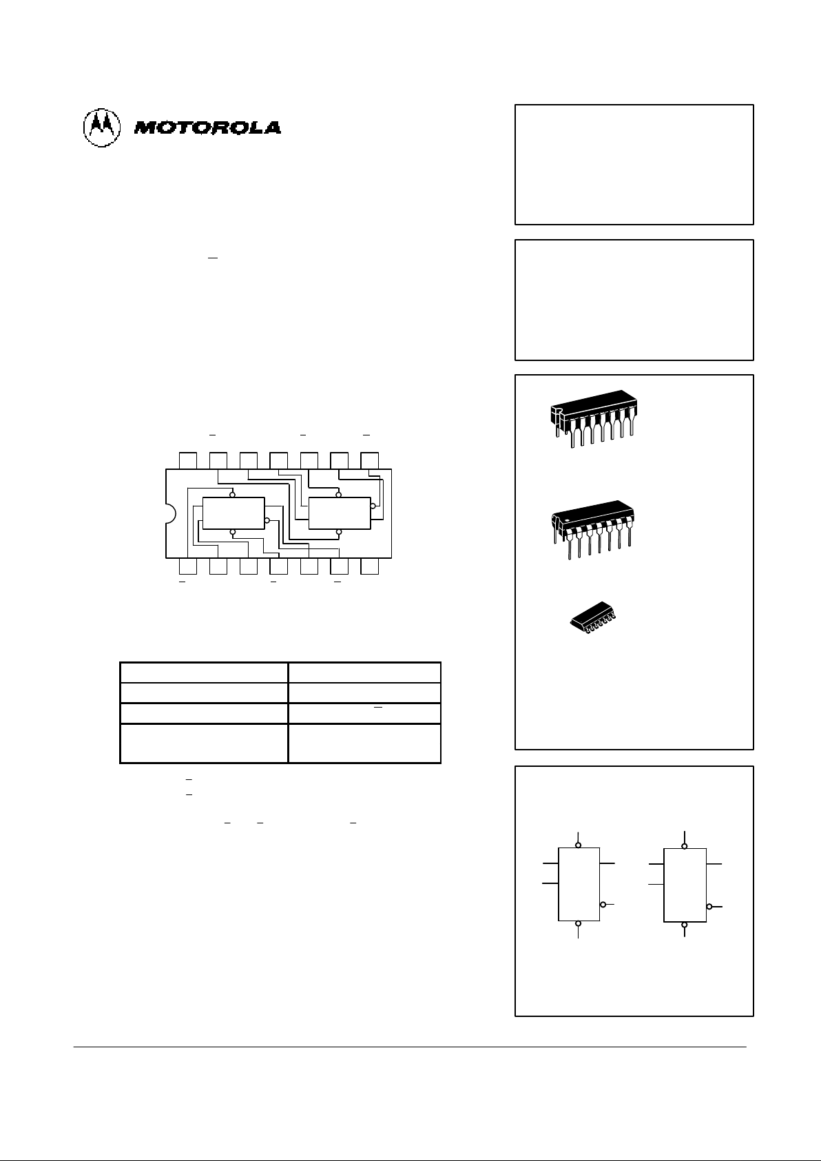
1314 12 11 10 9 8
21 3 4 5 6 7
GND
VCCC
D2D2
CP2SD2Q2Q
2
C
D1D1CP1SD1Q1Q1
CONNECTION DIAGRAM
CP
1
D
1
S
D1
C
D1
Q
1
Q
1
D
2
CP
2
C
D2
S
D2
Q
2
Q
2
FUNCTION TABLE (Each Half)
Input Outputs
@ t
n
@ tn + 1
D Q Q
L L H
H H L
H = HIGH Voltage Level
L = LOW Voltage Level
tn = Bit time before clock pulse
tn + 1 = Bit time after clock pulse
J SUFFIX
CERAMIC
CASE 632-08
N SUFFIX
PLASTIC
CASE 646-06
D SUFFIX
SOIC
CASE 751A-02
MC54FXXJ Ceramic
MC74FXXN Plastic
MC74FXXD SOIC
MC54/74F74
DUAL D-TYPE POSITIVE
EDGE-TRIGGERED FLIP-FLOP
FAST SCHOTTKY TTL
14
1
14
1
ORDERING INFORMATION
14
1
LOGIC SYMBOL
4
5
6
3
2
1
10
12
11
8
9
13
VCC = PIN 14
GND = PIN 7
S
D1
D
1
CP
1
Q
1
Q
1
C
D1
S
D2
D
2
CP
2
Q
2
Q
2
C
D2
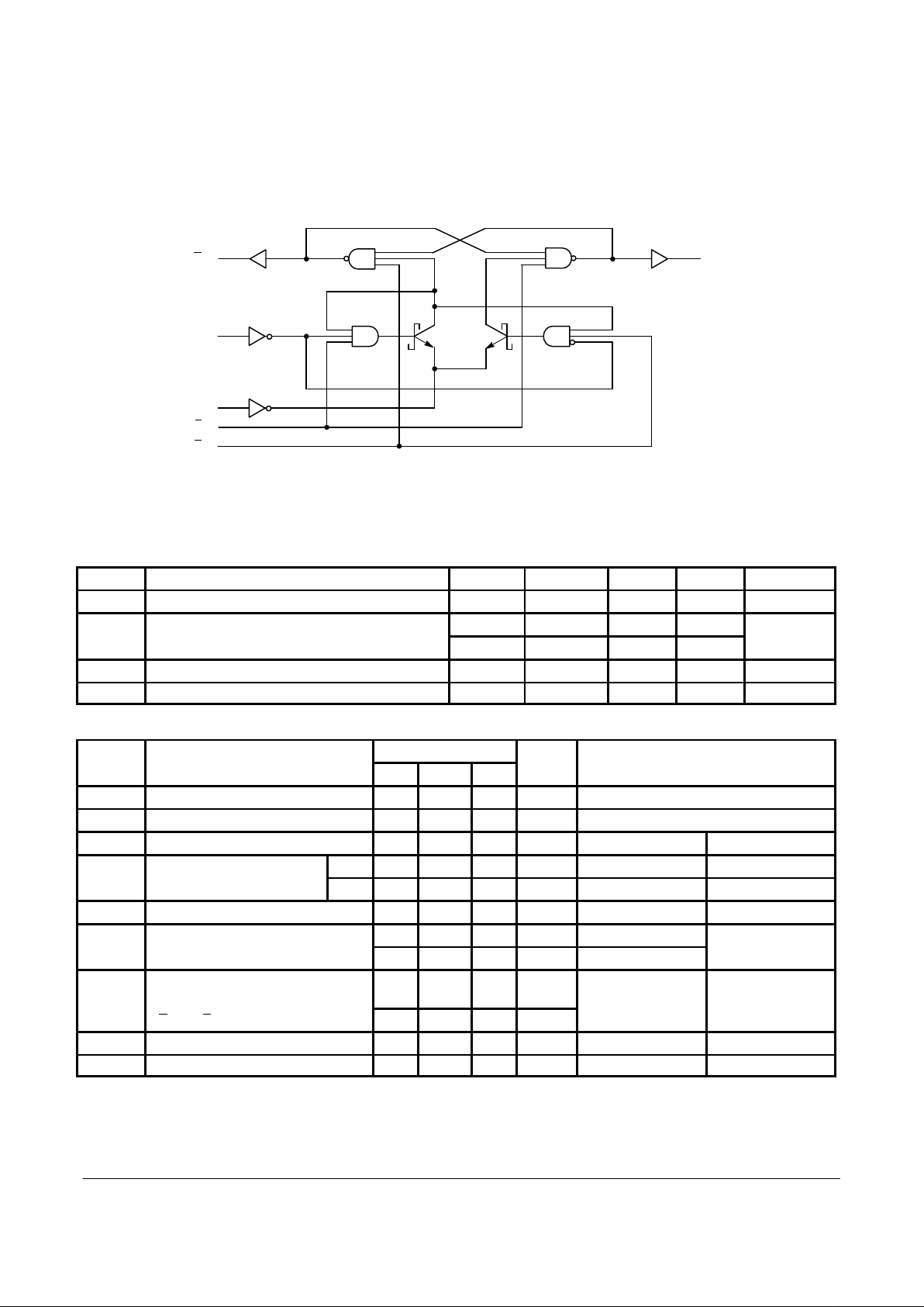
Asynchronous Inputs:
LOW Input to SD sets Q to HIGH level
LOW Input to CD sets Q to LOW level
Clear and Set are independent of clock
Simultaneous LOW on CD and SD makes both Q and Q HIGH
4-34
FAST AND LS TTL DATA
MC54/74F74
Q
S
D
Q
D
CP
C
D
LOGIC DIAGRAM
NOTE:
This diagram is provided only for the understanding of logic operations and should not be used to estimate propagation delays.
GUARANTEED OPERATING RANGES
Symbol Parameter Min Typ Max Unit
V
CC
Supply Voltage 54, 74 4.50 5.0 5.50 V
T
A
Operating Ambient Temperature Range
54 –55 25 125
°C
A
74 0 25 70
I
OH
Output Current — High 54, 74 –1.0 mA
I
OL
Output Current — Low 54, 74 20 mA
DC CHARACTERISTICS OVER OPERATING TEMPERATURE RANGE (unless otherwise specified)
Limits
Symbol Parameter Min Typ Max Unit Test Conditions
V
IH
Input HIGH Voltage 2.0 V Guaranteed Input HIGH Voltage
V
IL
Input LOW Voltage 0.8 V Guaranteed Input LOW Voltage
V
IK
Input Clamp Diode Voltage –1.2 V IIN = –18 mA VCC = MIN
54, 74 2.5 3.4 V IOH = –1.0 mA VCC = 4.50 V
V
OH
Output HIGH Voltage 74 2.7 3.4 V IOH = –1.0 mA VCC = 4.75 V
V
OL
Output LOW Voltage 0.35 0.5 V IOL = 20mA VCC = MIN
I
IH
Input HIGH Current 20 µA VIN = 2.7 V VCC = MAX
100 µA VIN = 7.0 V
I
IL
Input LOW Current
(CP and D Inputs)
–0.6 mA VIN = 0.5V VCC = MAX
(C
D
and SD Inputs)
–1.8 mA
I
OS
Output Short Circuit Current (Note 2) –60 –150 mA V
OUT
= 0 V VCC = MAX
I
CC
Power Supply Current 10.5 16 mA VCP = 0 V VCC = MAX
NOTES:
1. For conditions shown as MIN or MAX, use the appropriate value specified under guaranteed operating ranges.
2. Not more then one output should be shorted at a time, nor for more than 1 second.
 Loading...