4-241
FAST AND LS TTL DATA
Product Preview
OCTAL TRANSCEIVER/REGISTER
WITH 3-STATE OUTPUTS
These devices consist of bus transceiver circuits with 3-state D-type
flip-flops, and control circuitry arranged for multiplexed transmission of data
directly from the input bus or from the internal registers. Data on the A or B
bus will be clocked into the registers as the appropriate clock pin goes to a
high logic level. Output Enable (OE
) and DIR pins are provided to control the
transceiver function. In the transceiver mode, data present at the high
impedance port may be stored in either the A or the B register or in both. The
select controls can multiplex stored and real-time (transparent mode) data.
The direction control determines which bus will receive data when the enable
OE
is Active LOW. In the isolation mode (OE HIGH), A data may be stored
in the B register and/or B data may be stored in the A register.
• Independent Registers for A and B
• Multiplexed Real-Time and Stored Data
• Choice of True (F646) and Inverting (F648) Data Paths
• 3-State Outputs
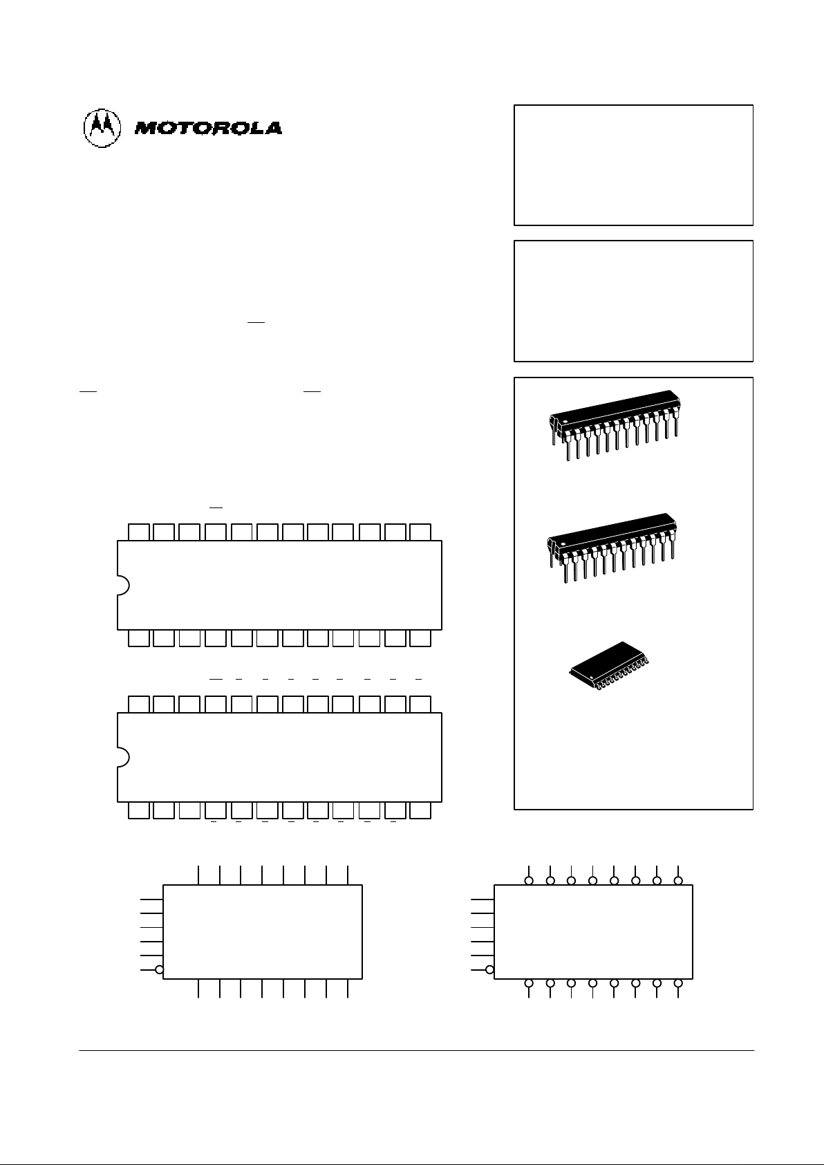
PIN ASSIGNMENTS
22 21 20 19 18 17
1 2 3 4 5 6
7
24 23
8
V
CC
CPAB
CPBA SBA OE
B
0
B
2
B
1
B
3
SAB DIR A0A1A2A3A
4
9 10
11
12
A5A6A7GND
16 15 14 13
B
4
B
6
B
5
B
7
F646
22 21 20 19 18 17
1 2 3 4 5 6
7
24 23
8
V
CC
CPAB
CPBA SBA OE
B
0
B
2
B
1
B
3
SAB DIR A
0A1A2A3A4
9 10
11
12
A
5A6A7
GND
16 15 14 13
B
4
B
6
B
5
B
7
F648
A0A1A2A3A4A5A6A
7
B0B1B2B3B4B5B6B
7
F646
CPAB
SAB
DIR
CPBA
SBA
OE
A0A1A2A3A4A5A6A
7
B0B1B2B3B4B5B6B
7
F648
CPAB
SAB
DIR
CPBA
SBA
OE
LOGIC SYMBOLS
1
2
3
23
22
21
20 19 18 17 16 15 14 13
4 5 6 7 8 9 10 11
20 19 18 17 16 15 14 13
1
2
3
23
22
21
4 5 6 7 8 9 10 11
This document contains information on a product under development. Motorola reserves the right to change or discontinue this product without notice.
MC54/74F646
MC54/74F648
OCTAL TRANSCEIVER/REGISTER
WITH 3-STATE OUTPUTS
FAST SCHOTTKY TTL
ORDERING INFORMATION
MC54FXXXJ Ceramic
MC74FXXXN Plastic
MC74FXXXDW SOIC
N SUFFIX
PLASTIC
CASE 724-03
DW SUFFIX
SOIC
CASE 751E-03
24
1
24
1
J SUFFIX
CERAMIC
CASE 758-01
24
1

4-242
FAST AND LS TTL DATA
MC54/74F646 • MC54/74F648
FUNCTION TABLE
Inputs Data I/O*
OE bar DIR CPAB CPBA SAB SBA A0–A
7
B0–B
7
Operation/Function
H
H
H
H
X
X
X
X
H or L
↑
X
↑
H or L
X
↑
↑
X
X
X
X
X
X
X
X
Input
Input
Input
Input
Input
Input
Input
Input
Isolation
Store An Data in A Register
Store Bn Data in B Register
Store An/Bn Data in A/B Register
L
L
L
L
H
H
H
H
X
↑
H or L
↑
X
X
X
X
L
L
H
H
X
X
X
X
Input
Input
Input
Input
Output
Output
Output
Output
An to Bn — Real Time (Transparent Mode)
Store An Data in A Register
A Register to Bn (Stored Mode)
Clock An Data to Bn and into A Register
L
L
L
L
L
L
L
L
X
X
X
X
X
↑
H or L
↑
X
X
X
X
L
L
H
H
Output
Output
Output
Output
Input
Input
Input
Input
Bn to An — Real Time (Transparent Mode)
Store Bn Data in B Register
B Register to An (Stored Mode)
Clock An Data to Bn and into B Register
*The data output function may be enabled or disabled by various signals at the OE bar and DIR inputs. Data input functions are always enabled; i.e., data at the
*bus pins will be stored on every low-to-high transition of the appropriate clock inputs.
H = HIGH voltage level
L = LOW voltage level
X = Don’t Care
↑ = Low-to-High transition
GUARANTEED OPERATING RANGES
Symbol Parameter Min Typ Max Unit
V
CC
DC Supply Voltage 54, 74 4.5 5.0 5.5 V
T
A
Operating Ambient Temperature Range
54
74
–55
0
25
25
125
70
°C
I
OH
Output Current High
54
74
—
—
—
—
–12
–15
mA
I
OL
Output Current Low
54
74
—
—
—
—
48
64
mA
 Loading...