

Motorola MC74F543DW, MC74F543N Datasheet
4-212
FAST AND LS TTL DATA
OCTAL REGISTERED
TRANSCEIVER,
NON-INVERTING, 3-STATE
The MC74F543 Octal Registered Transceivers contain two sets of data
flowing in either direction. Separate Latch Enable (LEAB
, LEBA) and Enable
(OEAB
, OEBA) inputs are provided for each register to permit independent
control of inputting and outputting in either direction of data flow. The
MC74F543 has a noninverting data path. The A outputs are guaranteed to
sink 20 mA while the B outputs are rated for 64 mA.
• Combines 74F245 and 74F373 Type Functions in One Chip
• 8-Bit Octal Transceiver
• Non-Inverting
• Back-to-Back Registers for Storage
• Separate Controls for Data Flow in Each Direction
• Glitchless Outputs During 3-State Power Up or Power Down Operation
• High Impedance Outputs in Power Off State
• A Outputs Sink 24 mA and Source 3.0 mA
• B Outputs Sink 64 mA and Source 15 mA
• See F544 for Inverting Version
• ESD Protection > 4000 Volts
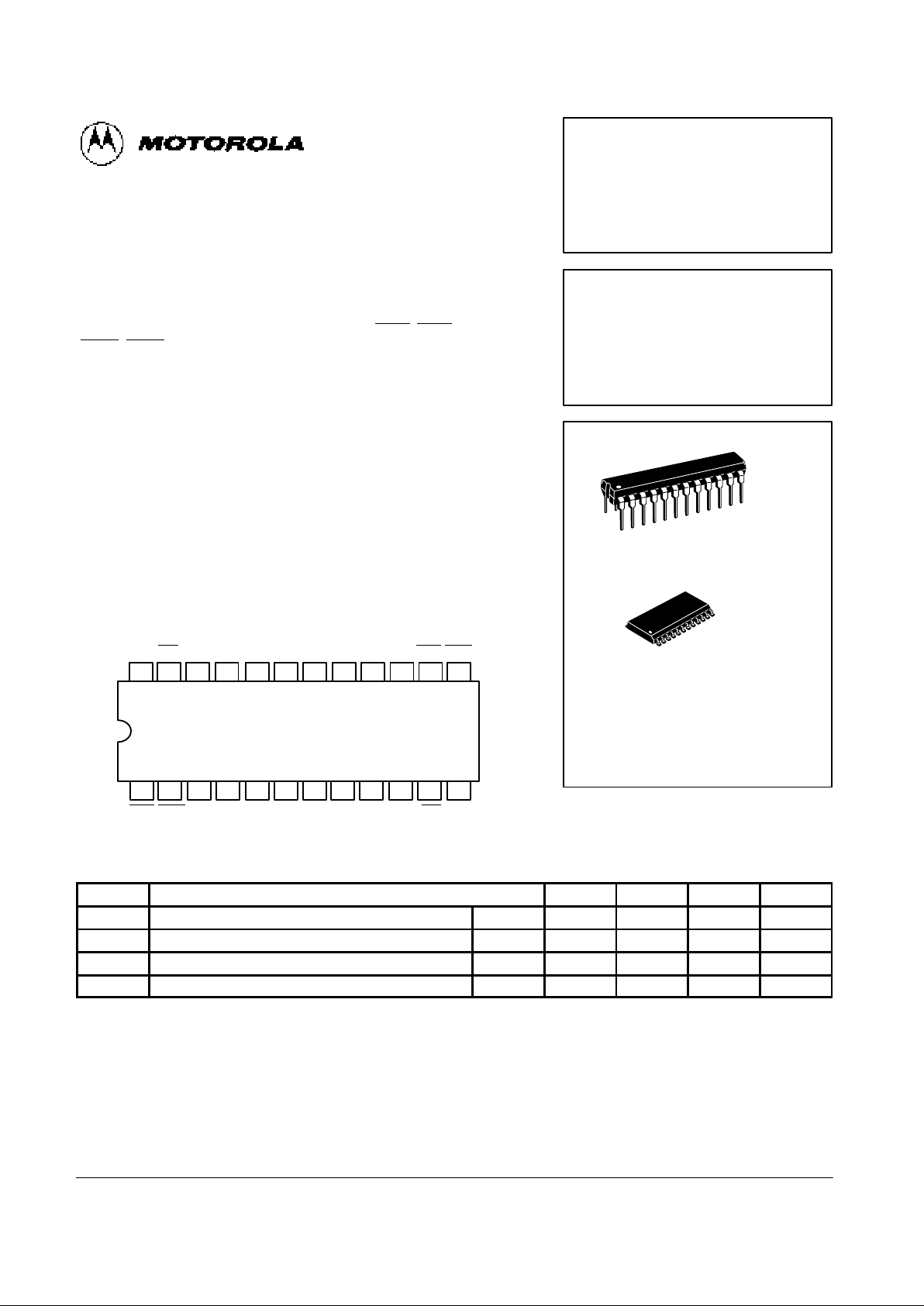
PIN ASSIGNMENT
18 17 16 15 14 13
1 2 3 4 5 6
7
20 19
8
B2
LEBA
B3 B4 B5 B6 LEABB7 OEAB
OEBA A0 A2 A3 A4 A5 A6
9 10
A7A1
11 12
22 2124 23
VCCEBA B0 B1
EAB
GND
GUARANTEED OPERATING RANGES
Symbol Parameter Min Typ Max Unit
V
CC
Supply Voltage 74 4.5 5.0 5.5 V
T
A
Operating Ambient Temperature Range 74 0 25 70 °C
I
OH
Output Current — High 74 –3.0/–15 mA
I
OL
Output Current — Low 74 24/64 mA
MC74F543
OCTAL REGISTERED
TRANSCEIVER,
NON-INVERTING, 3-STATE
FAST SCHOTTKY TTL
ORDERING INFORMATION
MC74FXXXN Plastic
MC74FXXXDW SOIC
N SUFFIX
PLASTIC
CASE 724-03
DW SUFFIX
SOIC
CASE 751E-03
24
1
24
1
4-213
FAST AND LS TTL DATA
MC74F543
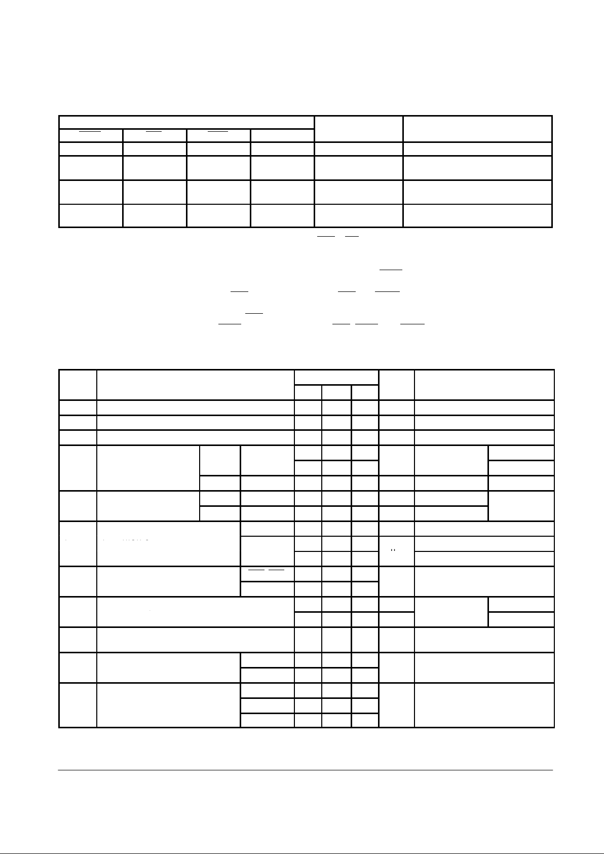
FUNCTION TABLE
Inputs
OEXX EXX LEXX Data
Outputs
Status
H X X X Z Outputs disabled
L
L
H
H
L
L
l
h
Z
Z
Outputs disabled
Data latched
L
L
L
L
H
H
l
h
L
H
Data latched
L
L
L
L
L
L
L
H
L
H
Transparent
H = HIGH voltage level: h = HIGH state must be present one set-up time before the LOW-to-HIGH transition of LEXX or EXX (XX = AB or BA): L = LOW V oltage Level:
I = LOW state must be present one set-up time before the LOW-to-HIGH transition of LEXX
or EXX (XX = AB or BA): X = Don’t care: Z = HIGH impedance state.
FUNCTIONAL DESCRIPTION
The MC74F543 contains two sets of eight D-type latches,
with separate input and controls for each set. For data flow
from A to B, for example, the A-to-B Enable (EAB
) Input must
be LOW in order to enter data from A0–A7 or take data from
B0–B7, as indicated in the Function Table. With EAB LOW, a
LOW signal on the A-to-B Latch Enable (LEAB
) input makes
the A-to-B latches transparent; a subsequent LOW-to-HIGH
transition of the LEAB
signal puts the A latches in the storage
mode and their outputs no longer change with the A inputs.
With EAB
and OEAB both LOW, the 3-State B output buffers
are active and reflects the data present at the output of the A
latches. Control of data flow from B to A is similar, but using
the EBA
, LEBA, and OEBA inputs.
DC CHARACTERISTICS OVER OPERATING TEMPERATURE RANGE
(unless otherwise specified)
Limits
Symbol
Parameter
Min Typ Max
Unit
Test Conditions
V
IH
Input HIGH Voltage 2.0 V Guaranteed Input HIGH Voltage
V
IL
Input LOW Voltage 0.8 V Guaranteed Input LOW Voltage
V
IK
Input Clamp Diode Voltage –0.73 –1.2 V VCC = MIN, IIN = –18 mA
2.4
VCC = 4.5 V
V
OH
Output HIGH Voltage
A0–A7
74
2.7 3.4
V
IOH = –3.0 mA
VCC = 4.75 V
OH
B0–B7 74 2.0 V IOH = –15 mA VCC = 4.5 V
A0–A7 74 0.35 0.5 V IOL = 24 mA
VOLOutput LOW Voltage
B0–B7 74 0.4 0.55 V IOL = 64 mA
VCC = MIN
I/O Pins 1.0 mA VCC = MAX, VIN = 5.5 V
I
IH
Input HIGH Current
100
VCC = MAX, VIN = 7.0 V
IH
Control Pins
20
µA
VCC = MAX, VIN = 2.7 V
EAB, EBA –1.2
IILInput LOW Current
Other Inputs –0.6
mA
VCC = MAX, VIN = 0.5 V
Off-State Output Current,
70 µA
V
OUT
= 2.7 V
I
OZH
Off-State Output Current,
High-Level Voltage Applied
1.0 mA
VCC = MAX
V
OUT
= 5.5 V
I
OZL
Off-State Output Current,
Low-Level Voltage Applied
–600 µA VCC = MAX, V
OUT
= 0.5 V
AnOutputs –60 –150
IOSOutput Short Circuit Current (Note 2)
BnOutputs –100 –225
mA
VCC = MAX, V
OUT
= 0 V
I
CCH
70 100
I
CC
Total Supply Current
I
CCL
95 125
mA VCC = MAX
CC
I
CCZ
95 125
CC
= MAX
NOTES:
1. For conditions shown as MIN or MAX, use the appropriate value specified under recommended operating conditions for the applicable device type.
2. Not more than one output should be shorted at a time, nor for more than 1 second.
 Loading...