

Motorola MC74F538DW, MC74F538N, MC54F538J Datasheet
4-206
FAST AND LS TTL DATA
1-OF-8 DECODER
WITH 3-STATE OUTPUTS
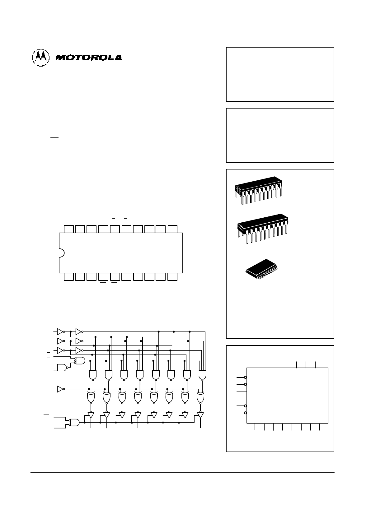
The MC54/74F538 decoder/demultiplexer accepts three Address (A0–A2)
input signals and decodes them to select one of eight mutually exclusive
outputs. A polarity control input (P) determines whether the outputs are active
LOW or active HIGH. A HIGH Signal on either of the active LOW Output
Enable (OE
) inputs forces all outputs to the high impedance state. Two active
HIGH and two active LOW input enables are available for easy expansion to
1-of-32 decoding with four packages, or for data demultiplexing to 1-of-8 or
1-of-16 destinations.
• Output Polarity Control
• Data Demultiplexing Capability
• Multiple Enables for Expansion
• 3-State Outputs
• ESD Protection > 4000 Volts
CONNECTION DIAGRAM DIP (TOP VIEW)
18 17 16 15 14 13
1 2 3 4 5 6
7
20 19
8
V
CC
O
2
O3O4A2E
1
E
3
E
2
E
4
O1O
0
OE
2A0A1O5O6
9 10
GND
12 11
O
7
OE
1
P
MC54/74F538
1-OF-8 DECODER
WITH 3-STATE OUTPUTS
FAST SCHOTTKY TTL
ORDERING INFORMATION
MC54FXXXJ Ceramic
MC74FXXXN Plastic
MC74FXXXDW SOIC
20
1
J SUFFIX
CERAMIC
CASE 732-03
20
1
N SUFFIX
PLASTIC
CASE 738-03
20
1
DW SUFFIX
SOIC
CASE 751D-03
LOGIC SYMBOL
VCC = PIN 20
GND = PIN 10
P A0A1A
2
O0O1O2O3O4O5O6O
7
E
1
E
2
E
3
E
4
OE
1
OE
2
12 6 7 17
16
15
14
13
4
5
3 2 1 14 18 8 9 11
LOGIC DIAGRAM
A
2
A
1
A
0
E
1
E
2
E
3
E
4
OE
1
OE
2
O
0
O
2
O
4
O
7
P
O
1
O
3
O5O
6
Please note that this diagram is provided only for the understanding of logic operations and
should not be used to estimate propagation delays.
4-207
FAST AND LS TTL DATA
MC54/74F538
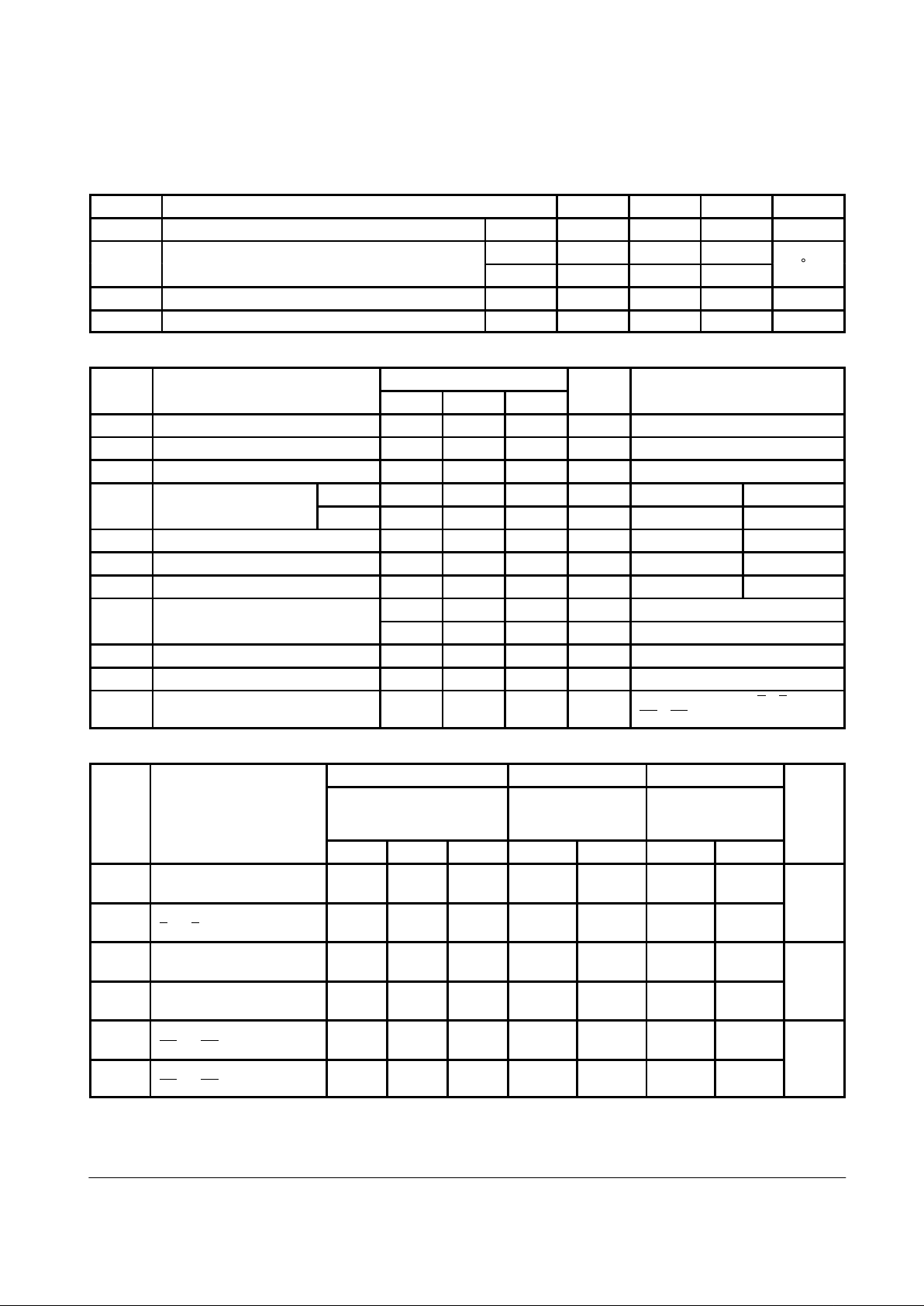
GUARANTEED OPERATING RANGES
Symbol Parameter Min Typ Max Unit
V
CC
Supply Voltage 54, 74 4.5 5.0 5.5 V
54 –55 25 125
TAOperating Ambient Temperature Range
74 0 25 70
°C
I
OH
Output Current — High 54, 74 –3.0 mA
I
OL
Output Current — Low 54, 74 24 mA
DC CHARACTERISTICS OVER OPERATING TEMPERATURE RANGE (unless otherwise specified)
Limits
Symbol
Parameter
Min Typ Max
Unit
Test Conditions
V
IH
Input HIGH Voltage 2.0 V Guaranteed Input HIGH Voltage
V
IL
Input LOW Voltage 0.8 V Guaranteed Input LOW Voltage
V
IK
Input Clamp Diode Voltage –1.2 V VCC = MIN, IIN = –18 mA
54, 74 2.4 V
IOH = –3.0 mA VCC = 4.5 V
VOHOutput HIGH Voltage
74 2.7 V
IOH = –3.0 mA VCC = 4.75 V
V
OL
Output LOW Voltage 0.5 V IOL = 24 mA VCC = MIN
I
OZH
Output OFF Current — HIGH 50 µA V
OUT
= 2.7 V VCC = MAX
I
OZL
Output OFF Current — LOW –50 µA V
OUT
= 0.5 V VCC = MAX
20 µA VCC = MAX, VIN = 2.7 V
IIHInput HIGH Current
0.1 mA VCC = MAX, VIN = 7.0 V
I
IL
Input LOW Current –0.6 mA VCC = MAX, VIN = 0.5 V
I
OS
Output Short Circuit Current (Note 2) –60 –150 mA VCC = MAX, V
OUT
= 0 V
I
CCZ
Power Supply Current 37 56 mA
VCC = MAX: A0–A2, E
1
, E2 = GND
OE
1
, OE2, E3, E4, P = HIGH
AC CHARACTERISTICS
54/74F 54F 74F
TA= +25°C
VCC= +5.0 V
CL= 50pF
TA = –55 to +125′C
VCC = 5.0 V ± 10%
CL= 50pF
TA = 0 to 70°C
VCC = 5.0 V ± 10%
CL= 50pF
Symbol
Parameter
Min Typ Max Min Max Min Max
Unit
t
PLH
t
PHL
Propagation Delay
An to O
n
4.0
3.0
11
7.5
13
12.5
4.0
3.0
17
16.5
4.0
3.0
14
13.5
t
PLH
t
PHL
Propagation Delay
E1 or E2 to O
n
4.0
3.0
8.5
6.5
12
12
3.5
3.0
15
14.5
3.5
3.0
13
12.5
ns
t
PLH
t
PHL
Propagation Delay
E3 or E4 to O
n
6.5
4.0
11
10
12.5
12.5
5.5
3.5
15.5
15
5.5
3.5
13.5
13
t
PLH
t
PHL
Propagation Delay
P to O
n
4.5
3.5
11.5
11
15
11.5
4.0
3.5
18.5
12.5
4.0
3.5
16.5
12
ns
t
PZH
t
PZL
Output Enable Time
OE
1
or OE2 to O
n
2.5
4.0
5.5
9.0
9.5
13.5
2.0
4.0
13
16
2.0
4.0
11
15
t
PHZ
t
PLZ
Output Disable Time
OE1 or OE2 to O
n
1.0
1.0
4.0
5.0
6.0
8.5
1.0
1.0
8.0
10.5
1.0
1.0
7.0
9.5
ns
 Loading...