

Motorola MC74F399D, MC74F399N, MC54F399J Datasheet
4-192
FAST AND LS TTL DATA
QUAD 2-PORT REGISTER
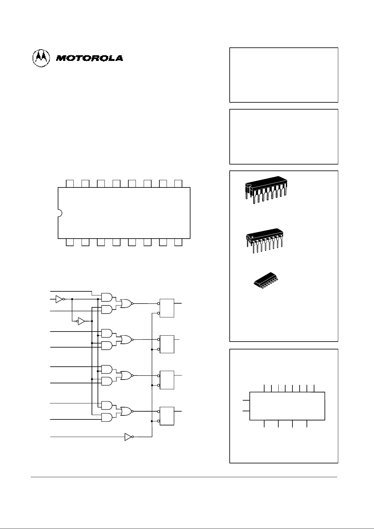
The MC54/74F399 is the logical equivalent of a quad 2-input multiplexer
feeding into four edge-triggered flip flops. A common Select input determines
which of the two 4-bit words is accepted. The selected data enters the flipflops on the rising edge of the clock. The MC54/74F399 is the 16-pin version
of the MC54/74F398, with only the Q outputs of the flip-flops available.
• Select Inputs from Two Data Sources
• Fully Positive Edge-Triggered Operation
6 7 81 2 3 4 5
10111314 12 91516
V
CCQdI0dI1dI1c
Q
c
I
0c
I
0aS
Q
a
I
1aI1b
Q
b
I
0b
CONNECTION DIAGRAM (TOP VIEW)
CP
GND
LOGIC DIAGRAM
NOTE:
This diagram is provided only for the understanding of logic operations and
should not be used to estimate propagation delays.
D
CP
Q
a
Q
b
Q
c
Q
d
I
0a
S
I
1a
I
0b
I
1b
I
0c
I
1c
I
0d
I
1d
CP
D
CP
D
CP
D
CP
J SUFFIX
CERAMIC
CASE 620-09
N SUFFIX
PLASTIC
CASE 648-08
16
1
16
1
ORDERING INFORMATION
MC54FXXXJ Ceramic
MC74FXXXN Plastic
MC74FXXXD SOIC
16
1
D SUFFIX
SOIC
CASE 751B-03
LOGIC SYMBOL
QUAD 2-PORT REGISTER
FAST SCHOTTKY TTL
MC54/74F399
I0a I1a I0b I1b I0c I1c I0d I
1d
S
CP
Q
a
Qb Q
c
Qd
3 4 6 5 11 12 14 13
2 7 10 15
1
9
VCC = PIN 16
GND = PIN 8
4-193
FAST AND LS TTL DATA
MC54/74F399
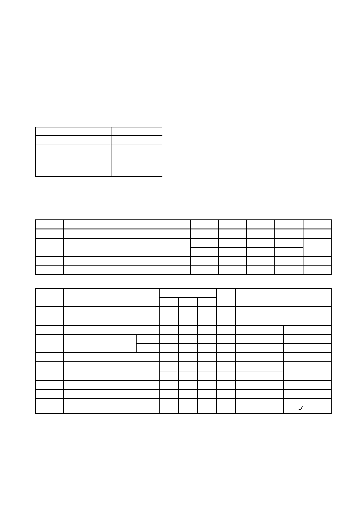
FUNCTIONAL DESCRIPTION
The MC54/74F398 is a high-speed quad 2-port register. It
will select four bits of data from either of two sources (Ports)
under control of a common Select input (S). The selected data
is transferred to a 4-bit output register synchronous with the
LOW-to-HIGH transition of the Clock input (CP). The 4-bit D-
type output register is fully edge-triggered. The Data inputs
(I0x, I1x) and Select input (S) must be stable only a setup time
prior to and hold time after the LOW-to-HIGH transition of the
Clock input for predictable operation.
Inputs Output
S
I
0
I
1
Q
I
I
h
h
I
h
X
X
X
X
I
h
L
H
L
H
H = HIGH Voltage Level
L = LOW Voltage Level
h = HIGH Voltage Level one setup time prior to the LOW-to-HIGH clock transition
I = LOW Voltage Level one setup time prior to the LOW-to-HIGH clock transition
X = Don’t Care
FUNCTION TABLE
GUARANTEED OPERATING RANGES
Symbol Parameter Min Typ Max Unit
V
CC
Supply Voltage 54, 74 4.5 5.0 5.5 V
T
A
Operating Ambient Temperature Range 54 –55 25 125 °C
74 0 25 70
I
OH
Output Current High 54, 74 – 1.0 mA
I
OL
Output Current Low 54, 74 20 mA
DC CHARACTERISTICS OVER OPERATING TEMPERATURE RANGE (unless otherwise specified)
Limits
Symbol Parameter Min Typ Max Unit Test Conditions
V
IH
Input HIGH Voltage 2.0 V Guaranteed Input HIGH Voltage
V
IL
Input LOW Voltage 0.8 V Guaranteed Input LOW Voltage
V
IK
Input Clamp Diode Voltage –1.2 V IIN = –18 mA VCC = MIN
V
OH
Output HIGH Voltage 54, 74 2.5 3.4 V IOH = – 1.0 mA VCC = 4.5 V
74 2.7 3.4 V IOH = – 1.0 mA VCC = 4.75 V
V
OL
Output LOW Voltage 0.35 0.5 V IOL = 20 mA VCC = MIN
I
IH
Input HIGH Current 20 µA VIN = 2.7 V VCC = MAX
100 µA VIN = 7.0 V
I
IL
Input LOW Current –0.6 mA VIN = 0.5 V VCC = MAX
I
OS
Output Short Circuit Current (Note 2) –60 –150 mA V
OUT
= 0 V VCC = MAX
I
CC
Power Supply Current 22 34 mA VCC = MAX VIN = GND
CP =
NOTES:
1. For conditions shown as MIN or MAX, use the appropriate value specified under guaranteed operating ranges.
2. Not more than one output should be shorted at a time, nor for more than 1 second.
 Loading...