

Motorola MC74F3893AFN Datasheet
4-273
FAST AND LS TTL DATA
QUAD FUTUREBUS
BACKPLANE TRANSCEIVER
(3 STATE + OPEN COLLECTOR)
The MC74F3893A is a quad backplane transceiver and is intended to be
used in very high speed bus systems.
The MC74F3893A interfaces to “Backplane Transceiver Logic” (BTL). BTL
features a reduced (1 V) voltage swing for lower power consumption and a series diode on the drivers to reduce capacitive loading (< 5 pF).
Incident wave switching is employed, therefore BTL propagation delays are
short. Although the voltage swing is much less for BTL, so is its receiver
threshold region, therefore noise margins are excellent.
BTL offers low power consumption, low ground bounce, reduced EMI and
crosstalk, low capacitive loading, superior noise margin and short propagation delays. This results in a high bandwidth, reliable backplane.
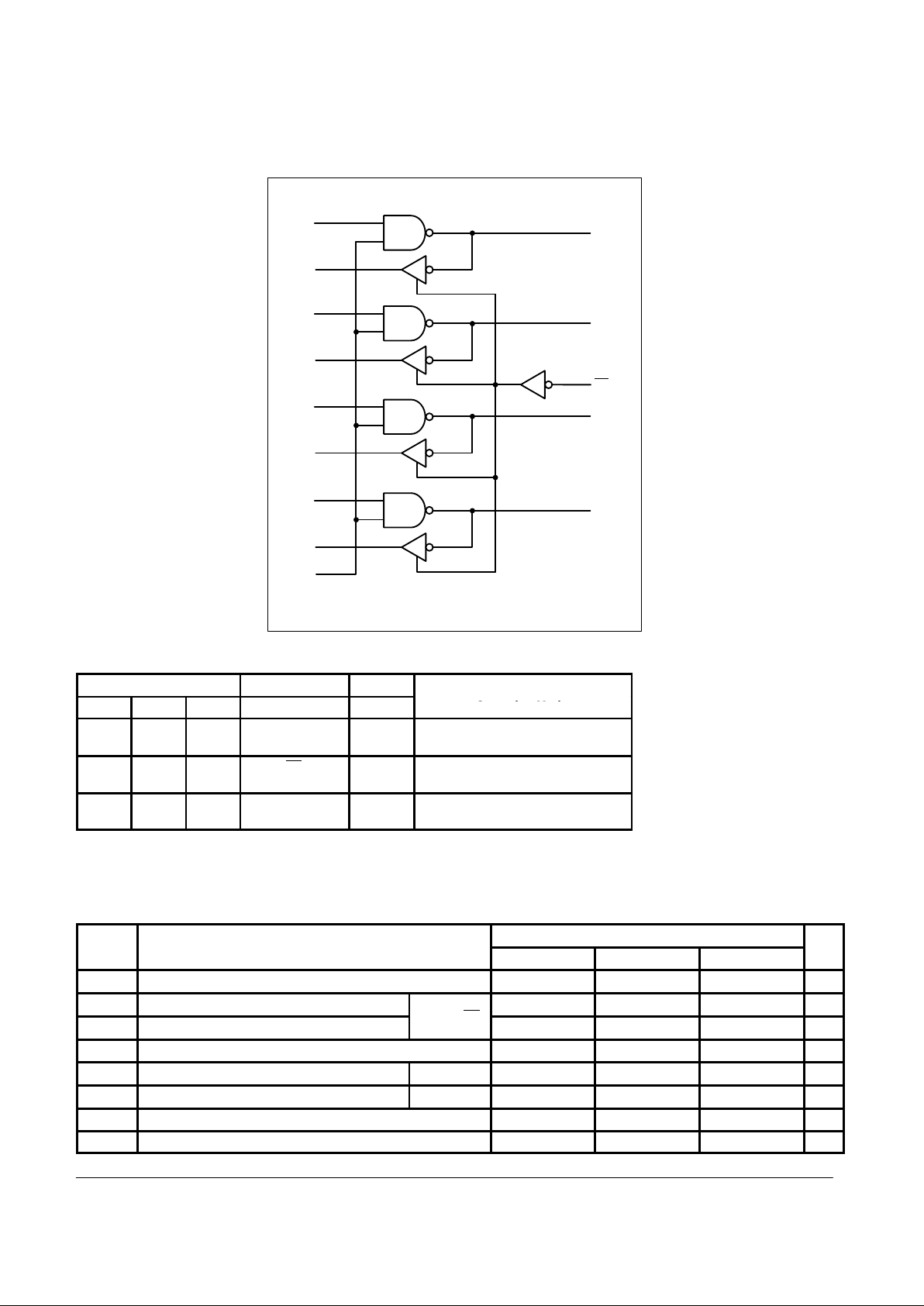
The MC74F3893A has four TTL outputs (Rn) on the receiver side with a
common Receive Enable input (RE
). It has four data inputs (Dn) which are also
TTL. These data inputs are NANDed with the Data Enable input (DE). The four
I/O pins (Bus side) are futurebus compatible, sink a minimum of 100 mA, and
are designed to drive heavily loaded backplanes with load impedances as low
as 10 ohms. All outputs are designed to be glitch-free during power up and
power down.
• Quad Backplane Transceiver
• Drives Heavily Loaded Backplanes with Equivalent Load Impedances
Down to 10 ohms
• Futurebus Drivers Sink 100 mA
• Reduced Voltage Swing (1 Volt) Produces Less Noise and Reduces
Power Consumption
• High Speed Operation Enhances Performance of Backplane Buses
and Facilitates Incident Wave Switching
• Compatible with IEEE 896 and IEEE 1194.1 Futurebus Standards
• Built-In Precision Band-Gap (BG) Reference Provides Accurate Re-
ceiver Threshold and Improved Noise Immunity
• Glitch-Free Power Up/Power Down Operation On All Outputs
• Pin and Function Compatible with NSC DS3893A and Signetics
74F3893
• Separate Bus Ground Returns for Each Driver to Minimize Ground
Noise
• MOS and TTL Compatible High Impedance Inputs
20
19
18 17 16 15 14
13
12
11
10
9
87654
3
2
1
I/O0I/O
1
I/O2I/O
3
BUS
GND
BUS
GND
BUS
GND
LOGIC
GND
BG
GND
V
CC
D
0
D
1
D
2
D
3
R
0
R
1
R
2
R
3
DE
RE
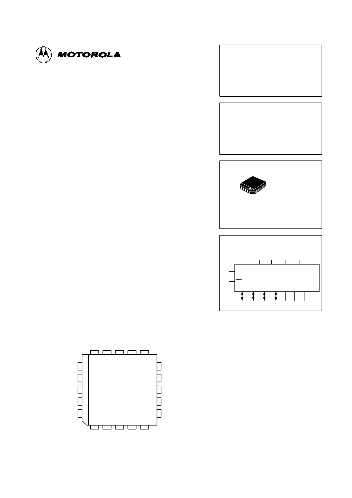
PINOUT: 20-LEAD PLCC (TOP VIEW)
MC74F3893A
QUAD FUTUREBUS
BACKPLANE TRANSCEIVER
(3 STATE + OPEN COLLECTOR)
FAST SCHOTTKY TTL
FN SUFFIX
PLASTIC
CASE 775-02
ORDERING INFORMATION
MC74FXXXXAFN Plastic
19
3
4
8
I/O0I/O1I/O2I/O
3
D0D1D2D
3
R0R1R2R
3
DE
RE
2 4 7 9
11
12
LOGIC SYMBOL
18 17 15 14 3 5 8 10
4-274
FAST AND LS TTL DATA
MC74F3893A
LOGIC DIAGRAM
I/O
0
I/O
1
I/O
2
I/O
3
D
0
D
1
D
2
D
3
R
0
R
1
R
2
R
3
DE
RE
VCC = PIN 1: LOGIC GND = PIN 6
BUS GND = PIN 13,16, 19: BG GND = PIN 20
2
3
4
5
7
8
9
10
11
14
15
12
17
18
FUNCTION TABLE
Inputs Input/Output Outputs
DE RE D
n
I/O
n
R
n
Operating Mode
H
H
L
L
L
H
H
L
L
H
Transmit to Bus
H
L
H
H
L
H
D
n
H
Z
Z
Receiver 3-State,
Transmit to Bus
L
L
L
L
X
X
H
L
L
H
Receive, I/On = Inputs
H = HIGH voltage level:
L = LOW voltage level:
X = Don’t care:
Z = HIGH impedance “Off” state.
RECOMMENDED OPERATING CONDITIONS
Limits
Symbol Parameter Min Typ Max Unit
V
CC
Supply Voltage 4.5 5.0 5.5 V
V
IH
High-Level Input Voltage
2.0 — — V
V
IL
Low-Level Input Voltage
Dn, DE, RE
— — 0.8 V
I
IK
Input Clamp Current — — –18 mA
V
TH
Bus Input Threshold I/On Only 1.475 1.550 1.625 V
I
OH
Output Current High Rn Only — — –3.0 mA
I
OL
Output Current Low — — 100 mA
T
A
Operating Ambient Temperature Range 0 — 70 °C
 Loading...