

4-104
FAST AND LS TTL DATA
4-BIT PARALLEL
ACCESS SHIFT REGISTER
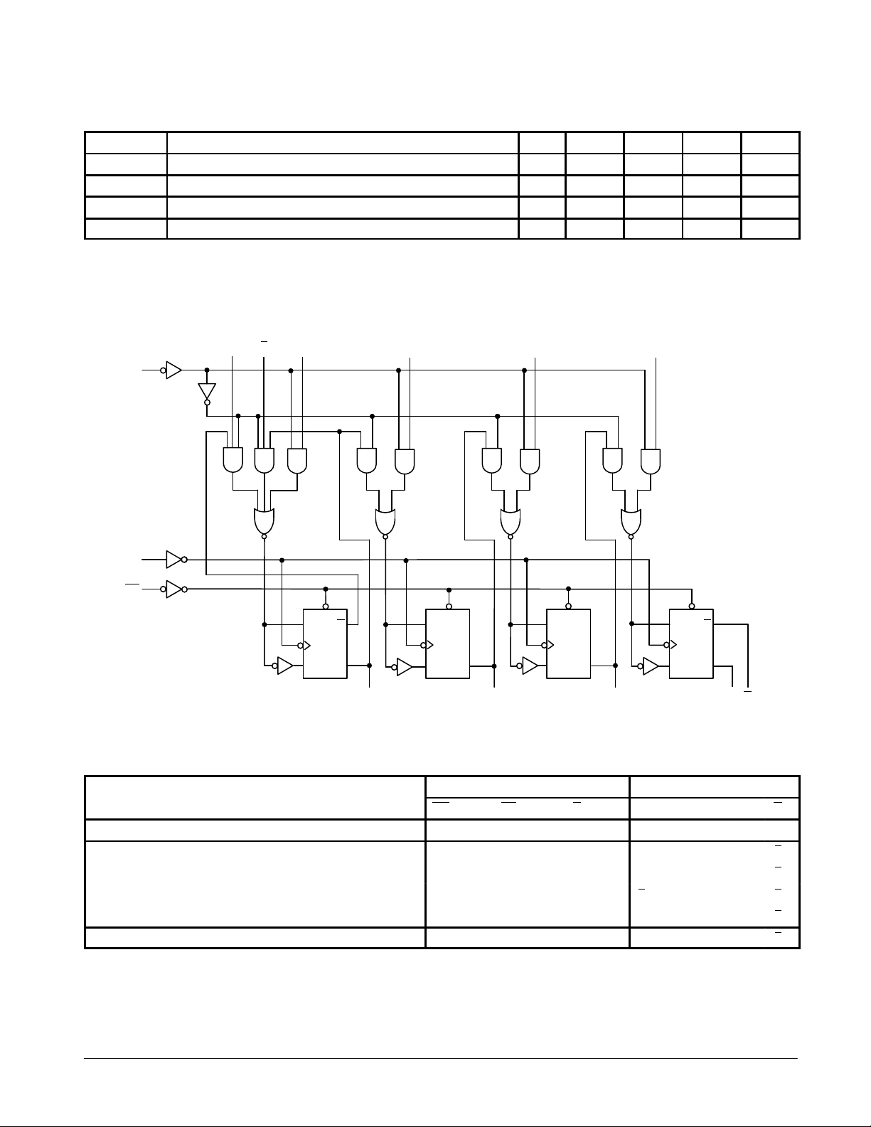
The functional characteristics of the MC74F195 4-Bit Parallel Access Shift
Register are indicated in the Logic Diagram and Function Table. The device
is useful in a wide variety of shifting, counting, and storage applications. It performs serial, parallel, serial-to-parallel, or parallel-to-serial data transfers at
very high speeds.
The MC74F195 operates in two primary modes, shift right (Q0-Q1) and parallel load, which are controlled by the state of the Parallel Enable (PE
) input.
Serial data enters the first flip-flop (Q0) via the J and K
inputs when the PE
input is HIGH, and is shifted 1 bit in the direction Q0-Q1-Q2-Q3 following each
LOW-to-HIGH clock transition. The J and K
inputs provide the flexibility of the
JK
type input is made for special applications, and by tying the two pins together the simple D-type input is made for general applications. The device appears as four common clocked D flip-flops when the PE
input is LOW. After
the LOW-to-HIGH clock transition, data on the parallel inputs (D0-D3) is transferred to the respective Q0-Q3 outputs. Shift left operation (Q3-Q2) can be
achieved by tying the Qn outputs to the D
n-1
inputs and holding the PE
input
LOW.
All parallel and serial data transfers are synchronous, occurring after each
LOW-to-HIGH clock transition. The MC74F195 utilizes edge-triggering;
therefore, there is no restriction on the activity of the J, K
, Dn, and PE inputs
for logic operation, other than the setup and hold time requirements.
A LOW on the asynchronous Master Reset (MR
) input sets all Q outputs
LOW, independent of any other input condition.
• Shift Right and Parallel Load Capability
• J-K (D-Type) Inputs to First Stage
• Complement Output from Last Stage
• Asynchronous Master Reset
1516 14 13 12 11 10
21 3 4 5 6 7
V
CC
9
8
Q0Q1Q2Q3Q
3
CP PE
MR J K D0D1D2D3GND
MC74F195
4-BIT PARALLEL
ACCESS SHIFT REGISTER
FAST SCHOTTKY TTL
J SUFFIX
CERAMIC
CASE 620-09
N SUFFIX
PLASTIC
CASE 648-08
16
1
16
1
ORDERING INFORMATION
MC74FXXXJ Ceramic
MC74FXXXN Plastic
MC74FXXXD SOIC
16
1
D SUFFIX
SOIC
CASE 751B-03
LOGIC SYMBOL
PE D0 D1 D2 D
3
J
K
CP
MR Q0 Q1 Q2 Q
3
Q
3
VCC = PIN 16
GND = PIN 8
9 5 6 7
2
3
10
11
1 15 14 13 12
4
CONNECTION DIAGRAM DIP
4-105
FAST AND LS TTL DATA
MC74F195
GUARANTEED OPERATING RANGES
Symbol Parameter Min Typ Max Unit
V
CC
Supply Voltage 74 4.5 5.0 5.5 V
T
A
Operating Ambient Temperature Range 74 0 25 70 °C
I
OH
Output Current High 74 –1.0 mA
I
OL
Output Current Low 74 20 mA
S
R
R
D
CP
Q S
R
R
D
CP
Q
Q
MR
CP
S
R
R
D
CP
Q
Q
0
Q
1
Q
2
Q3Q
3
D
3
D
2
D
1
D
0
J K
PE
S
R
R
D
CP
Q
Q
LOGIC DIAGRAM
FUNCTION TABLE
Inputs Outputs
Operating Modes MR CP PE J K DnQ0Q1Q2Q3Q
3
Asynchronous Reset L X X X X X L L L L H
Shift, Set First Stage H ↑ h h h X H q
0q1q2
q
2
Shift, Reset First Stage H ↑ h l l X L q
0q1q2
q
2
Shift, Toggle First Stage H ↑ h h l X q0q0q1q2q
2
Shift, Retain First Stage H ↑ h l h X q0q0q1q2q
2
Parallel Load H ↑ l X X dnd0d1d2d3d
3
H = HIGH Voltage Level
L = LOW Voltage Level
X = Don’t Care
dn (qn) = Lower case letters indicate the state of the referenced input (or output) one setup time prior to the LOW-to-HIGH clock transition.
↑ = LOW-to-HIGH clock transition
 Loading...