

4-101
FAST AND LS TTL DATA
4-BIT BIDIRECTIONAL
UNIVERSAL SHIFT REGISTER
The MC74F194 is a high-speed 4-bit bidirectional universal shift register. As
a high-speed multifunctional, sequential building block, it is useful in a wide
variety of applications. It may be used in serial-serial, shift left, shift right,
serial-parallel, parallel-serial, and parallel-parallel data register transfers. The
F194 is similar in operation to the S195 universal shift register, with added
features of shift left without external connections and hold (do nothing) modes
of operation.
• Typical Shift Frequency of 150 MHz
• Asynchronous Master Reset
• Hold (Do Nothing) Mode
• Fully Synchronous Serial or Parallel Data Transfers
FUNCTIONAL DESCRIPTION
The F194 contains four edge-triggered D flip-flops and the necessary
interstage logic to synchronously perform shift right, shift left, parallel load and
hold operations. Signals applied to the Select (S0, S1) inputs determine the
type of operation, as shown in the Function Table. Signals on the Select,
Parallel data (P0–P3) and Serial data (DSR, DSL) inputs can change when the
clock is in either state, provided only that the recommended setup and hold
times, with respect to the clock rising edge, are observed. A LOW signal on
Master Reset (MR
) overrides all other inputs and forces the outputs LOW.
14 13 12 11 10 9
1 2 3 4 5 6
7
16 15
8
V
CC
MR
Q0Q1Q2Q
3
S
1
CP S
0
DSRP0P1P2P3DSLGND
CONNECTION DIAGRAM
FUNCTION TABLE
Operating
Inputs Outputs
Operating
Mode
MR S1S0D
SRDSLPnQ0Q1Q2Q3
Reset L X X X X X L L L L
Hold H I I X X X q0q1q2q
3
H h I X I X q1q2q3L
Shift Left
H h I X h X q1q2q3H
H I h I X X L q0q1q
2
Shift Right
H I h h X X H q0q1q
2
Parallel Load H h h X X pnp0p1p2p
3
I = LOW voltage level one setup time prior to the LOW-to-HIGH clock transition.
h = HIGH voltage level one setup time prior to the LOW-to-HIGH clock transition.
pn, qn = Lower case letters indicate the state of the referenced input or output one setup
time prior to the LOW-to-HIGH clock transition.
H = HIGH Voltage Level
L = LOW Voltage Level
X = Immaterial
MC74F194
4-BIT BIDIRECTIONAL
UNIVERSAL SHIFT REGISTER
FAST SCHOTTKY TTL
J SUFFIX
CERAMIC
CASE 620-09
N SUFFIX
PLASTIC
CASE 648-08
16
1
16
1
ORDERING INFORMATION
MC74FXXXJ Ceramic
MC74FXXXN Plastic
MC74FXXXD SOIC
16
1
D SUFFIX
SOIC
CASE 751B-03
LOGIC SYMBOL
VCC = PIN 16
GND = PIN 8
11 10 9
2
3
4
5
6
7
1
15
14
13
12
MR
Q
0
Q
1
Q
2
Q
3
D
SR
P
0
P
1
P
2
P
3
D
SL
CP S1S
0
4-102
FAST AND LS TTL DATA
MC74F194
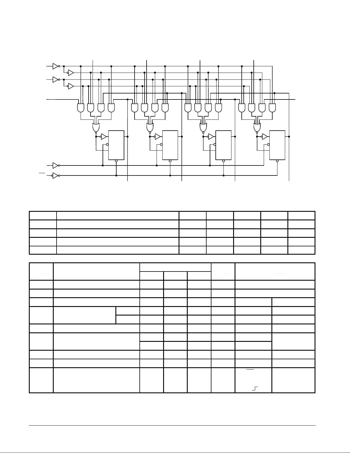
LOGIC DIAGRAM
S
1
S
0
D
SR
CP
MR
Q
0
Q
1
Q
2
Q
3
P
0
P
1
P
2
P
3
D
SR
S Q
0
CP
R
CLEAR
S Q
1
CP
R
CLEAR
S Q
2
CP
R
CLEAR
S Q
3
CP
R
CLEAR
Please note that this diagram is provided only for the understanding of logic operations and should not be used to estimate
propagation delays.
GUARANTEED OPERATING RANGES
Symbol Parameter Min Typ Max Unit
V
CC
Supply Voltage 74 4.5 5.0 5.5 V
T
A
Operating Ambient Temperature Range 74 0 25 70 °C
I
OH
Output Current — High 74 –1.0 mA
I
OL
Output Current — Low 74 20 mA
DC CHARACTERISTICS OVER OPERATING TEMPERATURE RANGE (unless otherwise specified)
Limits
Symbol
Parameter
Min Typ Max
Unit
Test Conditions
V
IH
Input HIGH Voltage 2.0 V Guaranteed Input HIGH Voltage
V
IL
Input LOW Voltage 0.8 V Guaranteed Input LOW Voltage
V
IK
Input Clamp Diode Voltage –1.2 V IIN = –18 mA VCC = MIN
74 2.5 3.4 V IOH = –1.0 mA VCC = 4.5 V
VOHOutput HIGH Voltage
74 2.7 3.4 V IOH = –1.0 mA VCC = 4.75 V
V
OL
Output LOW Voltage 0.35 0.5 V IOL = 20 mA VCC = MIN
20 µA VIN = 2.7 V
IIHInput HIGH Current
100 µA VIN = 7.0 V
VCC = MAX
I
IL
Input LOW Current –0.6 mA VIN = 0.5 V VCC = MAX
I
OS
Output Short Circuit Current (Note 2) –60 –150 mA V
OUT
= 0 V VCC = MAX
I
CC
Power Supply Current 33 46 mA
Sn, MR, DSR,
DSL = 4.5 V
Pn = Gnd,
CP =
VCC = MAX
NOTES:
1. For conditions such as MIN or MAX, use the appropriate value specified under guaranteed operating ranges.
2. Not more than one output should be shorted at a time, nor for more than 1 second.
 Loading...