

Motorola MC74F175D, MC74F175N, MC54F175J Datasheet
4-89
FAST AND LS TTL DATA
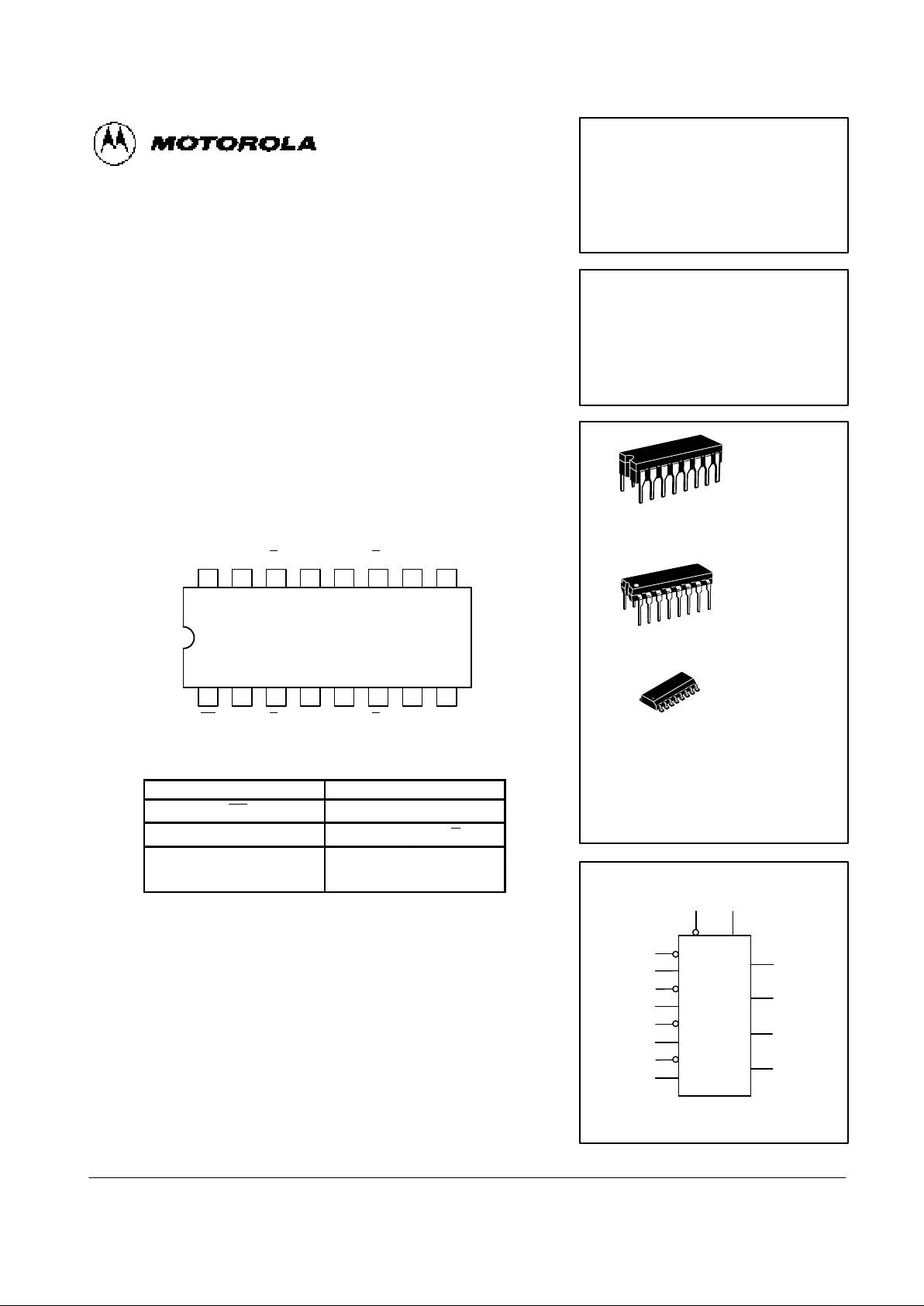
QUAD D FLIP-FLOP
The MC54/74F175 is a high-speed quad D flip-flop. The device is useful for
general flip-flop requirements where both true and complementary outputs
are required and clock and clear inputs are common to all flip-flops. The information on the D inputs is stored during the LOW-to-HIGH clock transition.
Both true and complemented outputs of each flip-flop are provided. A Master
Reset input resets all flip-flops, independent of the Clock or D inputs when
LOW.
• Four Edge-triggered D-type Inputs
• Buffered Positive Edge-triggered Common Clock
• Buffered Asynchronous Common Reset
• True and Complementary Outputs
• ESD
>
4000 Volts
CONNECTION DIAGRAM DIP (TOP VIEW)
1516 14 13 12 11 10
21 3 4 5 6 7
V
CC
9
8
Q3Q
3D3D2Q2Q2
CP
MR
Q0Q
0D0D1Q1Q1
GND
FUNCTION TABLE
Inputs Outputs
@ tn, MR = H @ tn + 1
D
n
Q
n
Q
n
L L H
H H L
tn = Bit time before clock positive-going transition
tn + 1 = Bit time after clock positive-going transition
H = HIGH Voltage Level
L = LOW Voltage Level
MC54FXXXJ Ceramic
MC74FXXXN Plastic
MC74FXXXD SOIC
MC54/74F175
QUAD D FLIP-FLOP
FAST SCHOTTKY TTL
J SUFFIX
CERAMIC
CASE 620-09
N SUFFIX
PLASTIC
CASE 648-08
16
1
16
1
ORDERING INFORMATION
16
1
D SUFFIX
SOIC
CASE 751B-03
LOGIC SYMBOL
1 9
4
5
12
13
3
2
6
7
11
10
14
15
D
2
D
1
D
0
Q
2
Q
1
Q
0
CPMR
D
3
Q
3
Q
3
Q
2
Q
1
Q
0
VCC = PIN 16
GND = PIN 8
4-90
FAST AND LS TTL DATA
MC54/74F175
D
CP
D
CP
D
CP
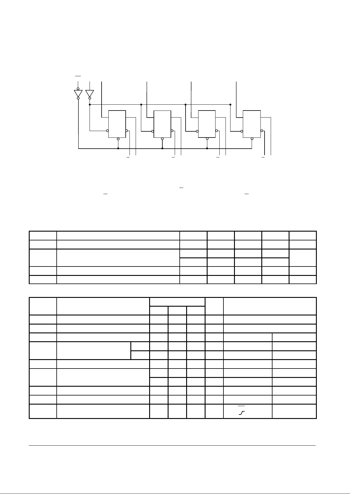
LOGIC DIAGRAM
D
3
D
1
D
0
D
2
Q
3
CPMR
Q
CD
Q
CD
Q
CD
D Q
CP
CD
Q
3
Q2Q
2
Q1Q
1
Q0Q
0
Q Q Q Q
NOTE:
This diagram is provided only for the understanding of logic operations and should not be used to estimate propagation delays.
FUNCTIONAL DESCRIPTION
The F175 consists of four edge-triggered D flop-flops with
individual D inputs and Q and Q outputs. The Clock and
Master Reset are common. The four flip-flops will store the
state of their individual D inputs, one setup time before, on the
LOW-to-HIGH clock (CP) transition, causing individual Q and
Q
outputs to follow. A LOW input on the Master Reset (MR) will
force all Q outputs LOW and Q
outputs HIGH independent of
Clock or Data inputs. The F175 is useful for general logic
applications where a common Master Reset and Clock are
acceptable.
GUARANTEED OPERATING RANGES
Symbol Parameter Min Typ Max Unit
V
CC
Supply Voltage 54, 74 4.5 5.0 5.5 V
T
A
Operating Ambient Temperature Range
54 –55 25 125 °C
A
74 0 25 70
I
OH
Output Current — High 54, 74 –1.0 mA
I
OL
Output Current — Low 54, 74 20 mA
DC CHARACTERISTICS OVER OPERATING TEMPERATURE RANGE (unless otherwise specified)
Limits
Symbol Parameter Min Typ Max Unit Test Conditions
V
IH
Input HIGH Voltage 2.0 V Guaranteed Input HIGH Voltage
V
IL
Input LOW Voltage 0.8 V Guaranteed Input LOW Voltage
V
IK
Input Clamp Diode Voltage –1.2 V IIN = –18 mA VCC = MIN
V
OH
Output HIGH Voltage 54, 74 2.5 3.4 V IOH = – 1.0 mA VCC = 4.50 V
74 2.7 3.4 V IOH = – 1.0 mA VCC = 4.75 V
V
OL
Output LOW Voltage 0.35 0.5 V IOL = 20 mA VCC = MIN
I
IH
Input HIGH Current 20 µA VIN = 2.7 V VCC = MAX
100 µA VIN = 7.0 V VCC = MAX
I
IL
Input LOW Current –0.6 mA VIN = 0.5 V VCC = MAX
I
OS
Output Short Circuit Current (Note 2) –60 –150 mA V
OUT
= 0 V VCC = MAX
I
CC
Power Supply Current 22.5 34 mA Dn = MR = 4.5 V
CP =
VCC = MAX
NOTES:
1. For conditions shown as MIN or MAX, use the appropriate value specified under guaranteed operating ranges.
2. Not more than one output should be shorted at a time, nor for more than 1 second.
 Loading...