

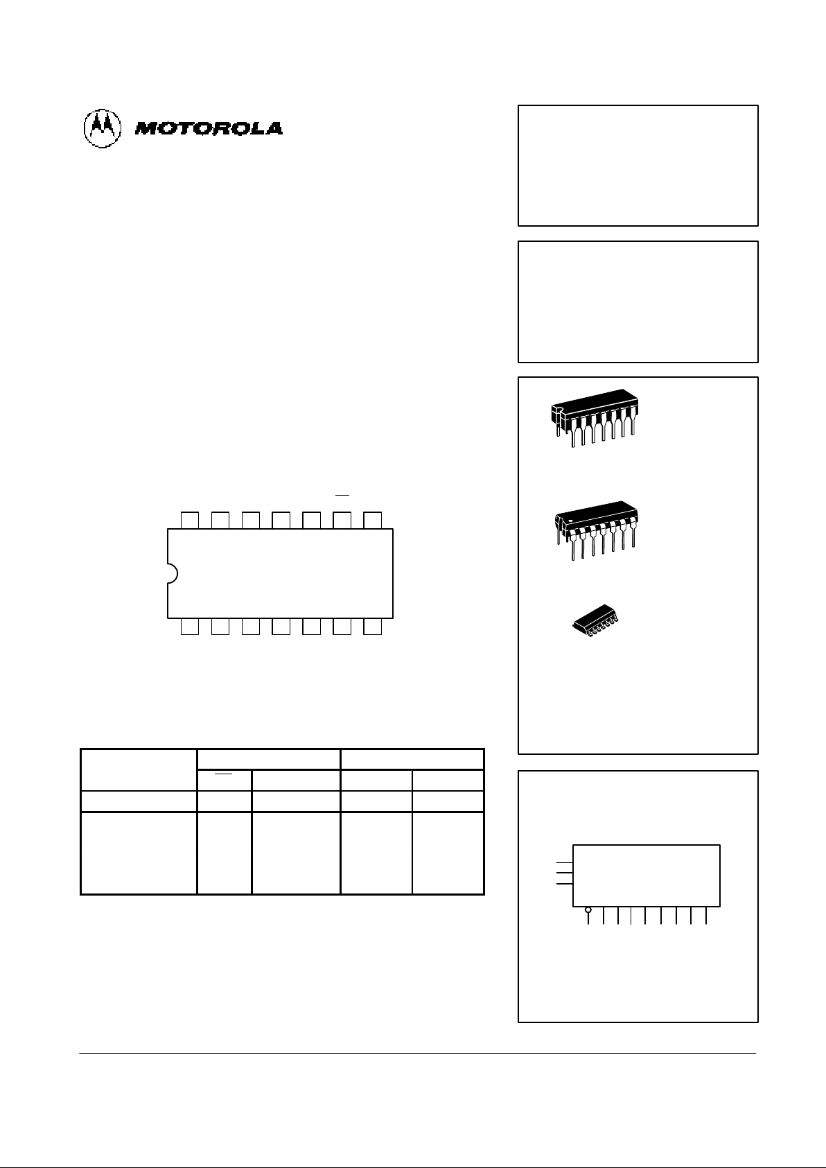
Motorola MC74F164AD, MC74F164AN, MC54F164AJ Datasheet
4-79
FAST AND LS TTL DATA
8-BIT SERIAL-IN, PARALLEL-OUT
SHIFT REGISTER
The MC54/74F164 is a high-speed 8-bit serial-in/parallel-out shift register .
Serial data is entered through a 2-input AND gate synchronous with the
LOW-to-HIGH transition of the clock. The device features an asynchronous
Master Reset which clears the register, setting all outputs LOW independent
of the clock.
• Typical Shift Frequency of 90 MHz
• Asynchronous Master Reset
• Gated Serial Data Input
• Fully Synchronous Data Transfers
MR
CP
CONNECTION DIAGRAM
1314 12 11 10 9 8
21 3 4 5 6 7
VCCQ7Q6Q5Q
4
A B Q0Q1Q2Q3GND
MODE SELECT TABLE
Inputs Outputs
Operating Mode MR A B Q
0
Q1 –Q
7
Reset (Clear) L X X L L–L
Shift H l l L q0–q
6
H l h L q0–q
6
H h l L q0–q
6
H h h H q0–q
6
H(h) = HIGH Voltage Levels
L(l) = LOW Voltage Levels
X = Don’t Care
qn = Lower case letters indicate the state of the referenced input or output one setup time prior to
the LOW-to-HIGH clock transition.
14
1
14
1
14
1
MC54/74F164
8-BIT SERIAL-IN, PARALLEL-OUT
SHIFT REGISTER
FAST SHOTTKY TTL
J SUFFIX
CERAMIC
CASE 632-08
N SUFFIX
PLASTIC
CASE 646-06
ORDERING INFORMATION
MC54FXXXJ Ceramic
MC74FXXXN Plastic
MC74FXXXD SOIC
D SUFFIX
SOIC
CASE 751A-02
LOGIC SYMBOL
CP
Q0Q
1
A
B
Q2Q4Q5Q6Q
7
MR Q
3
VCC = PIN 14
GND = PIN 7
8
2
1
9 3 4 5 6 13121110
4-80
FAST AND LS TTL DATA
MC54/74F164
MR
D
Q
C
D
D
Q
C
D
D
Q
C
D
D
Q
C
D
D
Q
C
D
D
Q
C
D
D
Q
C
D
A
B
CP
Q
0
Q
1
Q
2
Q
3
Q
4
Q
5
Q
6
Q
7
D
Q
C
D
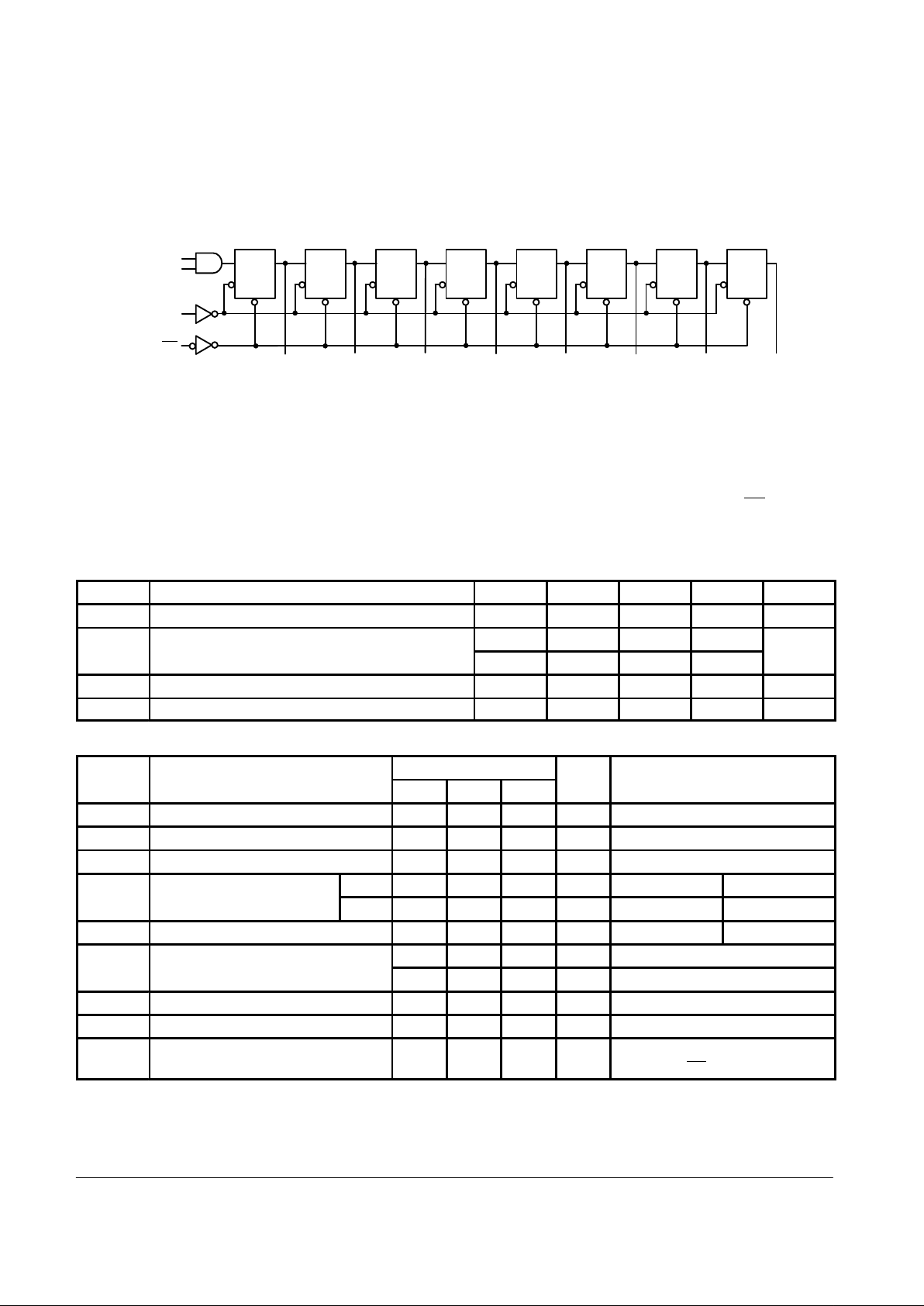
LOGIC DIAGRAM
FUNCTIONAL DESCRIPTION
The F164 is an edge-triggered 8-bit shift register with serial data entry and an output from each of the eight stages.
Data is entered serially through one of two inputs (A or B); either of these inputs can be used as an active HIGH Enable
for data entry through the other input. An unused input must
be tied HIGH.
Each LOW-to-HIGH transition on the Clock (CP) input
shifts data one place to the right and enters into Q0 the logical
AND of the two data inputs (A • B) that existed before the rising
clock edge. A LOW level on the Master Reset (MR
) input overrides all other inputs and clears the register asynchronously,
forcing all Q outputs LOW.
GUARANTEED OPERATING RANGES
Symbol Parameter Min Typ Max Unit
V
CC
Supply Voltage 54, 74 4.5 5.0 5.5 V
T
A
Operating Ambient Temperature Range 54 –55 25 125 °C
74 0 25 70
I
OH
Output Current High 54, 74 –1.0 mA
I
OL
Output Current Low 54, 74 20 mA
DC CHARACTERISTICS OVER OPERATING TEMPERATURE RANGE (unless otherwise specified)
Limits
Symbol Parameter Min Typ Max Unit Test Conditions
V
IH
Input HIGH Voltage 2.0 V Guaranteed Input HIGH Voltage
V
IL
Input LOW Voltage 0.8 V Guaranteed Input LOW Voltage
V
IK
Input Clamp Diode Voltage –1.2 V VCC = MIN, IIN = –18 mA
V
OH
Output HIGH Voltage 54, 74 2.5 V IOH = –1.0 mA VCC = MIN
74 2.7 V IOH = –1.0 mA VCC = 4.75 V
V
OL
Output LOW Voltage 0.5 V IOL = 20 mA VCC = MIN
I
IH
Input HIGH Current 20 µA VCC = MAX, VIN = 2.7 V
0.1 mA VCC = MAX, VIN = 7.0 V
I
IL
Input LOW Current –0.6 mA VCC = MAX, VIN = 0.5 V
I
OS
Output Short Circuit Current (Note 2) –60 –150 mA VCC = MAX, V
OUT
= 0 V
I
CC
Power Supply Current 35 55 mA A, B = GND, VCC = MAX
CP = HIGH, MR = GND
NOTES:
1. For conditions shown as MIN or MAX, use the appropriate value specified under recommended operating conditions for the applicable device type.
2. Not more than one output should be shorted at a time, nor for more than 1 second.
 Loading...