

Motorola MC74F160AN, MC74F160AD, MC54F160AJ Datasheet
4-71
FAST AND LS TTL DATA
SYNCHRONOUS PRESETTABLE
BCD DECADE COUNTER
The MC74F160A and MC74F162A are high-speed synchronous decade
counters operating in the BCD (8421) sequence. They are synchronously presettable for application in programmable dividers and have two types of Count
Enable inputs plus a T erminal Count output for versatility in forming synchronous multistage counters. The MC74F160A has an asynchronous Master Reset input that overrides all other inputs and forces the outputs LOW. The
MC74F162A has a Synchronous Reset input that overrides counting and parallel loading and allows the outputs to be simultaneously reset on the rising
edge of the clock.
• Synchronous Counting and Loading
• High-Speed Synchronous Expansion
• Typical Count Rate of 120 MHz
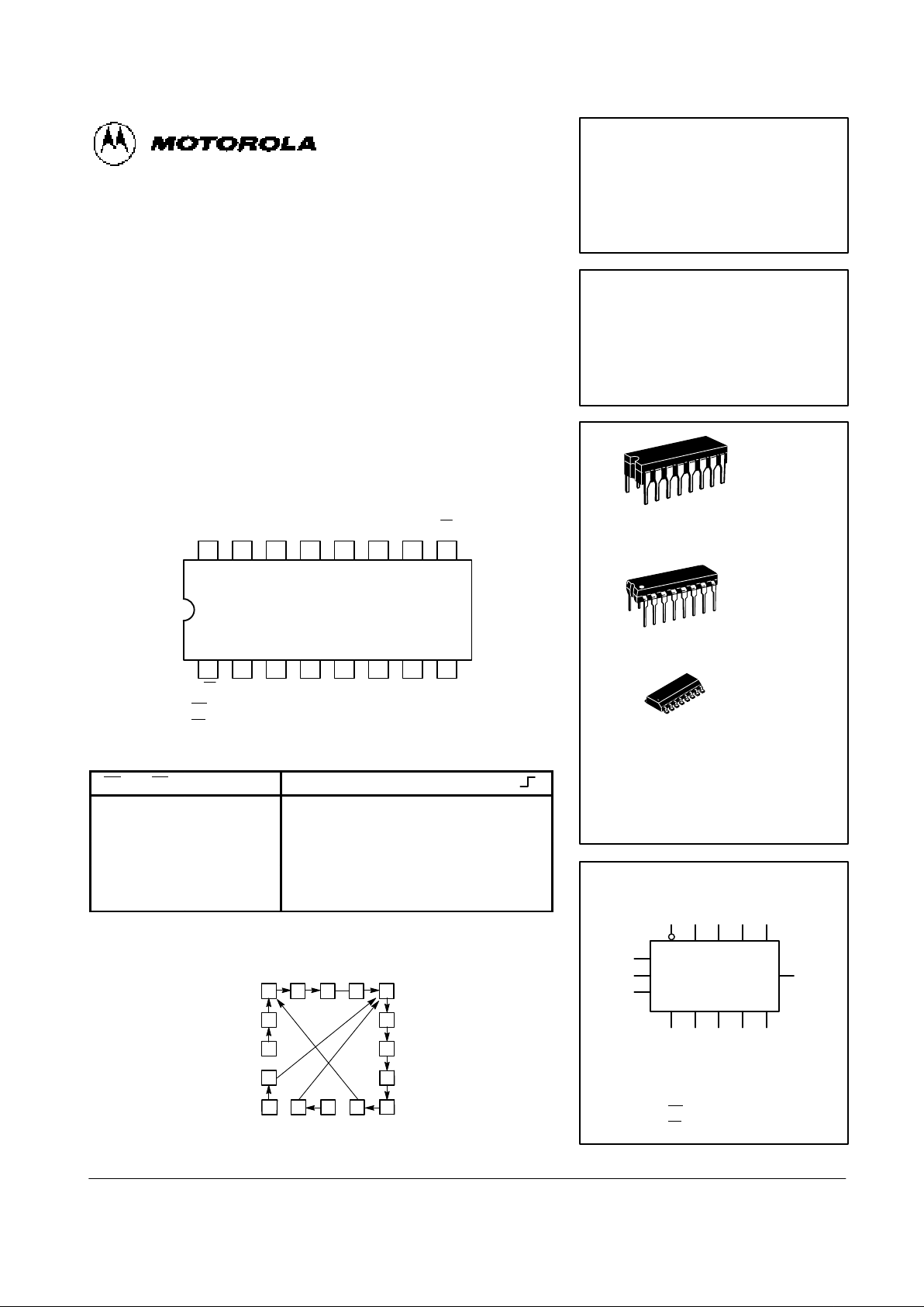
CONNECTION DIAGRAM
1516 14 13 12 11 10
21 3 4 5 6 7
V
CC
9
8
TC Q0Q1Q2Q3CET PE
*R CP P0P1P2P3CEP GND
*MR for MC74F160A
*SR for MC74F162A
FUNCTION TABLE
SR PE CET CEP ACTION ON THE RISING CLOCK EDGE ( )
L X X X Reset (Clear)
H L X X Load (Pn º Qn)
H H H H Count (Increment)
H H L X No Change (Hold)
H H X L No Change (Hold)
H = HIGH Voltage Level; L = LOW Voltage Level; X = Don’t Care
15
12
STATE DIAGRAM
1 2 3 4
5
6
7
8
91011
13
14
0
MC74F160A
MC74F162A
ORDERING INFORMATION
MC74FXXXAJ Ceramic
MC74FXXXAN Plastic
MC74FXXXAD SOIC
LOGIC SYMBOL
PE P
0
P
1
P3P
2
CEP
CET
CP
*R
Q
0
Q
1
Q2Q
3
TC
J SUFFIX
CERAMIC
CASE 620-09
N SUFFIX
PLASTIC
CASE 648-08
16
1
16
1
16
1
D SUFFIX
SOIC
CASE 751B-03
SYNCHRONOUS PRESETTABLE
BCD DECADE COUNTER
FAST SHOTTKY TTL
VCC = PIN 16
GND = PIN 8
1
15
7
14 13 12 11
9 3 4 5 6
10
2
*MR
for MC74F160A
*SR
for MC74F162A
4-72
FAST AND LS TTL DATA
MC74F160A • MC74F162A
CP
D
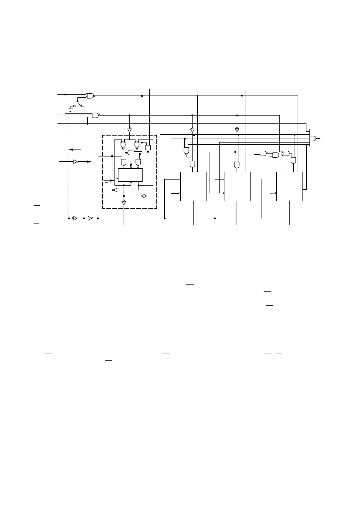
NOTE:
This diagram is provided only for the understanding of logic operations and should not be used to estimate propagation delays.
LOGIC DIAGRAM
DETAIL A DETAIL A
DETAIL A
DETAIL A
P
0
P
1
P
3
P
2
CEP
CET
CP
Q
0
Q
1
Q
2
Q
3
MR
(MC74F160A)
SR
(MC74F162A)
Q
0
Q
0
TC
CP
CP D
Q Q
C
D
MC74F160A
MC74F162A
MC74F162A
ONLY
MC74F160A
ONLY
PE
FUNCTIONAL DESCRIPTION
The MC74F160A and MC74F162A count modulo-10 in the
BCD (8421) sequence. From state 9 (HLLH) they increment
to state 0 (LLLL). The clock inputs of all flip-flops are driven in
parallel through a clock buffer. Thus, all changes of the Q outputs (except due to Master Reset of the MC74F160A) occur
as a result of, and synchronous with, the LOW-to-HIGH transition of the CP input signal. The circuits have four fundamental
modes of operation, in order of precedence: asynchronous reset (MC74F160A), synchronous reset (MC74F162A), parallel load, count-up and hold. Five control inputs — Master Reset (MR
, MC74F160A), Synchronous Reset (SR,
MC74F162A), Parallel Enable (PE
), Count Enable Parallel
(CEP) and Count Enable Trickle (CET) — determine the mode
of operation, as shown in the Function T able. A LOW signal on
MR
overrides all other inputs and asynchronously forces all
outputs LOW. A LOW signal on SR
overrides counting and
parallel loading and allows all outputs to go LOW on the next
rising edge of CP . A LOW signal on PE
overrides counting and
allows information on the Parallel Data (Pn) inputs to be
loaded into the flip-flops on the next rising edge of CP. With
PE
and MR (MC74F160A) or SR (MC74F162A) HIGH, CEP
and CET permit counting when both are HIGH. Conversely , a
LOW signal on either CEP or CET inhibits counting.
The MC74F160A and MC74F162A use D-type edge-trig-
gered flip-flops and changing the SR
, PE, CEP, and CET inputs when the CP is in either state does not cause errors, provided that the recommended setup and hold times, with
respect to the rising edge of CP, are observed.
 Loading...