

Motorola MC74F157AN, MC54F157AJ Datasheet
4-67
FAST AND LS TTL DATA
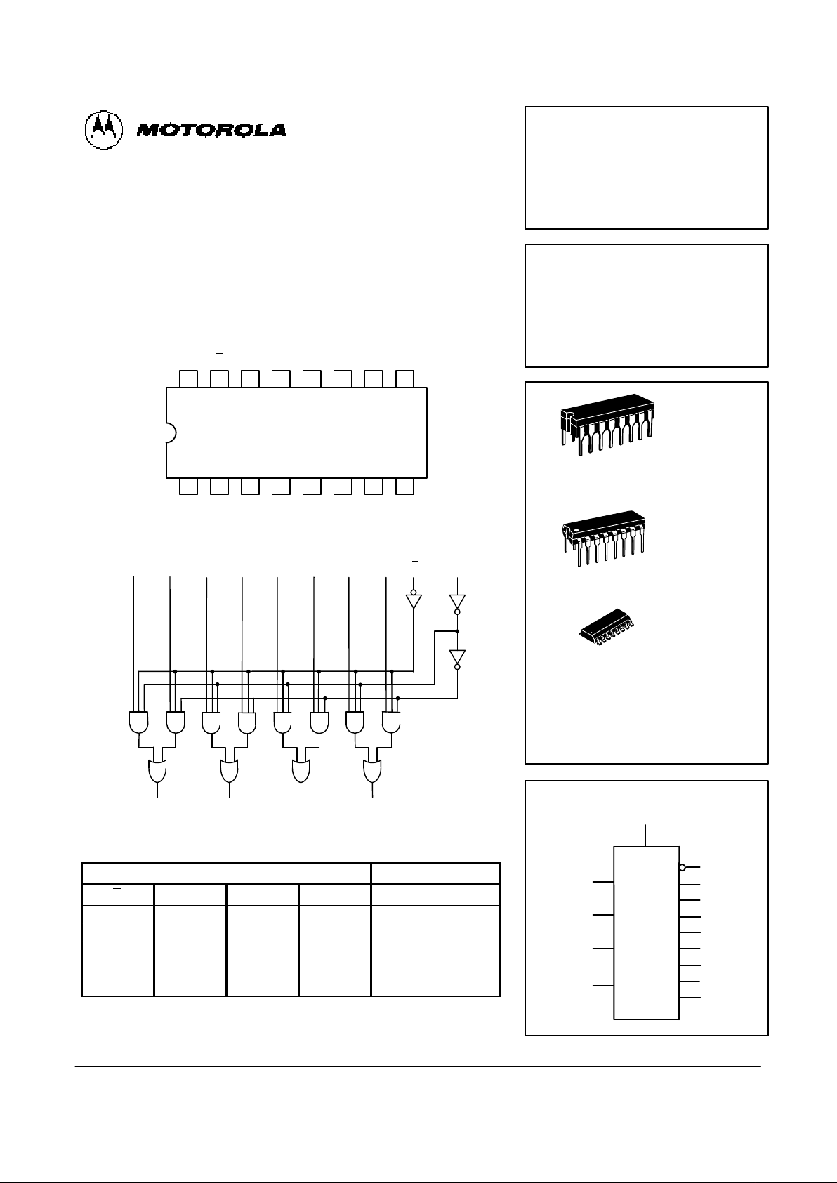
QUAD 2-INPUT MULTIPLEXER
The MC74F157A is a high-speed quad 2-input multiplexer. Four bits of data
from two sources can be selected using the common Select and Enable inputs. The four buffered outputs present the selected data in the true (non-inverted) form. The F157A can also be used to generate any four of the 16 different functions to two variables.
• AC Enhanced Version of the F157
Z
c
CONNECTION DIAGRAM DIP (TOP VIEW)
1516 14 13 12 11 10
21 3 4 5 6 7
V
CC
9
8
E
I0cI
1cZcI0dI1dZd
S I
0aI1aZaI0bI1bZb
GND
LOGIC DIAGRAM
I
0aI1aI0bI1bI0c
I
1b
I
1cI0d
SEI
1d
Z
a
Z
b
Z
d
FUNCTION TABLE
Inputs Output
E S I
0
I
1
Z
H X X X L
L H X L L
L H X H H
L L L X L
L L H X H
H = HIGH Voltage Level; L = LOW Voltage Level; X = Don’t Care
MC74FXXXJ Ceramic
MC74FXXXN Plastic
MC74FXXXD SOIC
MC74F157A
QUAD 2-INPUT
MULTIPLEXER
FAST SHOTTKY TTL
J SUFFIX
CERAMIC
CASE 620-09
N SUFFIX
PLASTIC
CASE 648-08
16
1
16
1
ORDERING INFORMATION
16
1
D SUFFIX
SOIC
CASE 751B-03
LOGIC SYMBOL
12
13
14
15
1
2
3
4
7
5
6
11
10
9
Z
a
Z
b
Zc
Z
d
I
1a
I
0a
E
I
0c
I
1c
I
1d
I
0d
I
0b
I
1b
VCC = PIN 16
GND = PIN 8
S
4-68
FAST AND LS TTL DATA
MC74F157A
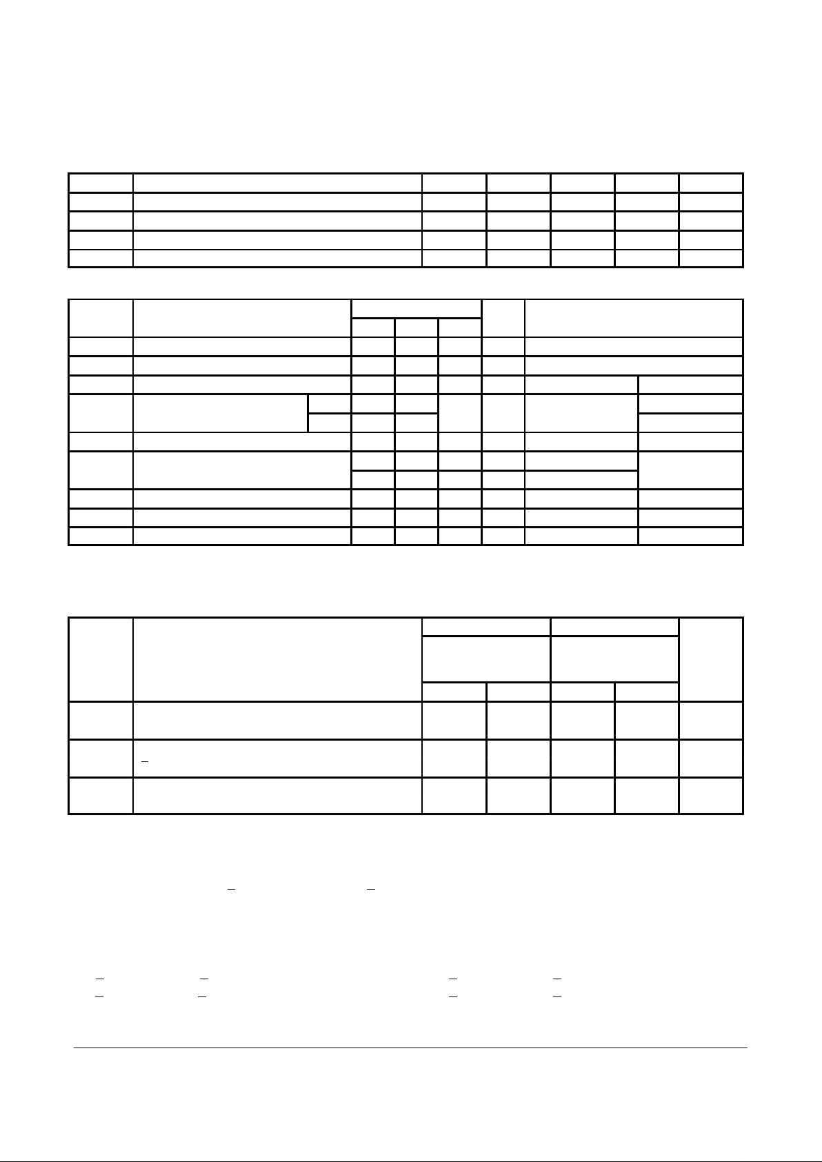
GUARANTEED OPERATING RANGES
Symbol Parameter Min Typ Max Unit
V
CC
Supply Voltage 74 4.5 5.0 5.5 V
T
A
Operating Ambient Temperature Range 74 0 25 70 °C
I
OH
Output Current — High 74 –1.0 mA
I
OL
Output Current — Low 74 20 mA
DC CHARACTERISTICS OVER OPERATING TEMPERATURE RANGE (unless otherwise specified)
Limits
Symbol Parameter Min Typ Max Unit Test Conditions
V
IH
Input HIGH Voltage 2.0 V Guaranteed Input HIGH Voltage
V
IL
Input LOW Voltage 0.8 V Guaranteed Input LOW Voltage
V
IK
Input Clamp Diode Voltage –1.2 V IIN = –18 mA VCC = MIN
V
OH
Output HIGH Voltage 74 2.7 3.4 V
IOH = –1.0 mA
VCC = 4.75 V
74 2.5 VCC = 4.50 V
V
OL
Output LOW Voltage 0.35 0.5 V IOL = 20 mA VCC = MIN
I
IH
Input HIGH Current 20
µA VIN = 2.7 V VCC = MAX
100 µA VIN = 7.0 V
I
IL
Input LOW Current –0.6 mA VIN = 0.5 V VCC = MAX
I
OS
Output Short Circuit Current (Note 2) –60 –150 mA V
OUT
= 0 V VCC = MAX
I
CC
Power Supply Current 15 23 mA All Inputs = 4.5 V VCC = MAX
NOTES:
1. For conditions shown as MIN or MAX, use the appropriate value specified under guaranteed operating ranges.
2. Not more than one output should be shorted at a time, nor for more than 1 second.
AC CHARACTERISTICS
74F 74F
TA = +25°C
VCC = +5.0 V
CL = 50 pF
TA = 0°C to 70°C
VCC = 5.0 V ±10%
CL = 50 pF
Symbol Parameter Min Max Min Max
Unit
t
PLH
Propagation Delay 3.5 10 3.5 11
ns
t
PHL
S to Z
n
3.0 7.0 3.0 8.0
t
PLH
Propagation Delay 3.5 9.5 3.5 11
ns
t
PHL
E to Z
n
2.5 6.5 2.5 7.0
t
PLH
Propagation Delay 2.0 6.0 2.0 6.5
ns
t
PHL
In to Z
n
2.5 5.5 2.0 7.0
FUNCTIONAL DESCRIPTION
The F157A is a quad 2-input multiplexer. It selects four bits
of data from two sources under the control of a common Select
input (S). The Enable input (E
) is active LOW. When E is
HIGH, all of the outputs (Z) are forced LOW regardless of all
other inputs. The F157A is the logic implementation of a
4-pole, 2-position switch where the position of the switch is determined by the logic levels supplied to the Select input. The
logic equations for the outputs are shown below:
Za = E
• (I1a • S + I0a • S)
Zc = E
• (I1c • S + I0c • S)
A common use of the F157A is the moving of data from two
groups of registers to four common output busses. The particular register from which the data comes is determined by the
state of the Select input. A less obvious use is as a function
generator. The F157A can generate any four of the 16 dif ferent
functions of two variables with one variable common. This is
useful for implementing highly irregular logic.
Zb = E
• (I1b • S + I0b • S)
Zd = E
• (I1d • S + I0d • S)
 Loading...