

4-14
FAST AND LS TTL DATA
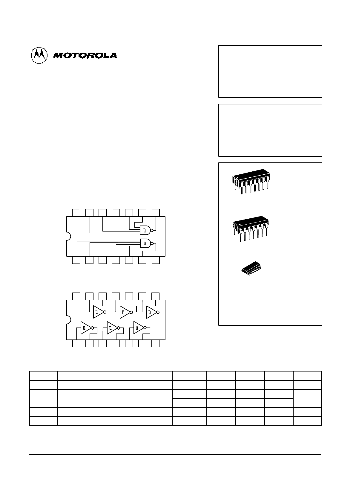
SCHMITT TRIGGERS DUAL 4-INPUT
NAND/HEX INVERTERS
The MC54/74F13 and MC54/74F14 contain logic gates/inverters which accept standard TTL input signals and provide standard TTL output levels. They
are capable of transforming slowly changing input signals into sharply defined, jitter-free output signals. Additionally, they have greater noise margin
than conventional inverters.
Each circuit contains a Schmitt trigger followed by a Darlington level shifter
and a phase splitter driving a TTL totem pole output. The Schmitt trigger uses
positive feedback to effectively speed up slow input transitions and provide
different input threshold voltages for positive and negative-going transitions.
This hysteresis between the positive-going and negative-going input thresholds (typically 800 mV) is determined internally by resistor ratios and is essentially insensitive to temperature and supply voltage variations.
V
CC
GND
1314 12 11 10 9 8
21 3 4 5 6 7
V
CC
GND
1314 12 11 10 9 8
21 3 4 5 6 7
MC54/74F13
MC54/74F14
LOGIC AND CONNECTION DIAGRAMS
D C N/C B A O
A B N/C C D O
A O A O A O
A O A O A O
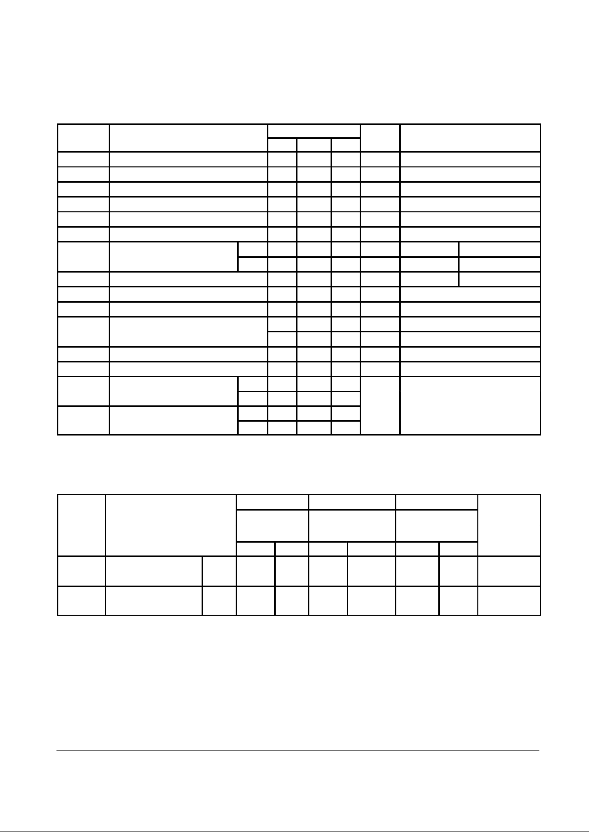
GUARANTEED OPERATING RANGES
Symbol Parameter Min Typ Max Unit
V
CC
Supply Voltage 54, 74 4.5 5.0 5.5 V
T
A
Operating Ambient Temperature Range 54 –55 25 125 °C
74 0 25 70
I
OH
Output Current — High 54, 74 –1.0 mA
I
OL
Output Current — Low 54, 74 20 mA
MC54FXXJ Ceramic
MC74FXXN Plastic
MC74FXXD SOIC
D SUFFIX
SOIC
CASE 751A-02
N SUFFIX
PLASTIC
CASE 646-06
J SUFFIX
CERAMIC
CASE 632-08
MC54/74F13
MC54/74F14
SCHMITT TRIGGERS
DUAL 4-INPUT
NAND/HEX INVERTERS
FAST SCHOTTKY TTL
14
1
14
1
ORDERING INFORMATION
14
1
4-15
FAST AND LS TTL DATA
MC54/74F13 • MC54/74F14
DC CHARACTERISTICS OVER OPERATING TEMPERATURE RANGE (unless otherwise specified)
Limits
Symbol Parameter Min Typ Max Unit Test Conditions
VT+ Positive-Going Threshold Voltage 1.5 2.0 V VCC = 5.0 V
VT– Negative-Going Threshold Voltage 0.7 1.1 V VCC = 5.0 V
VT+–VT– Hysteresis 0.4 0.8 V VCC = 5.0 V
V
IH
Input HIGH Voltage 2.0 V Guaranteed Input HIGH Voltage
V
IL
Input LOW Voltage 0.8 V Guaranteed Input LOW Voltage
V
IK
Input Clamp Diode Voltage –1.2 V VCC = MIN, IIN = –18 mA
V
OH
Output HIGH Voltage 54, 74 2.5 V IOH = –1.0 mA VCC = 4.5
74 2.7 V IOH = –1.0 mA VCC = 4.75
V
OL
Output LOW Voltage 0.5 V IOL = 20 mA VCC = MIN
IT+ Input Current at Positive-Going Threshold –0.14 mA VCC = 5.0 V, VIN = VT+
IT– Input Current at Negative-Going Threshold –0.18 mA VCC = 5.0 V, VIN = VT–
I
IH
Input HIGH Current
20 µA VCC = MAX, VIN = 2.7 V
0.1 mA VCC = MAX, VIN = 7.0 V
I
IL
Input LOW Current –0.6 mA VCC = MAX, VIN = 0.5 V
I
OS
Output Short Circuit Current (Note 2) –60 –150 mA VCC = MAX, V
OUT
= 0 V
I
CCH
Power Supply Current F13 4.5 8.5
Total, Output HIGH F14 13 22
I
CCL
Power Supply Current F13 7.0 10
mA
VCC = MAX
Total, Output LOW F14 23 32
NOTES:
1. For conditions shown as MIN or MAX, use the appropriate value specified under recommended operating conditions for the applicable device type.
2. Not more than one output should be shorted at a time, nor for more than 1 second.
AC CHARACTERISTICS (CL = 50 pF)
54/74F 54F 74F
TA = +25°C TA = –55°C to +125°C TA = 0°C to 70°C
VCC = +5.0 V
VCC = 5.0 V ± 10% VCC = 5.0 V ± 10%
Symbol Parameter Min Max Min Max Min Max Unit
t
PLH
Propagation Delay F13 3.5 7.0 3.5 9.0 3.5 8.0 ns
t
PHL
3.0 8.0 3.0 9.5 3.0 8.5
t
PLH
Propagation Delay F14 3.5 7.0 3.5 9.0 3.5 8.0 ns
t
PHL
3.0 6.5 3.0 8.0 3.0 7.0

4-16
FAST AND LS TTL DATA
MC54/74F13 • MC54/74F14
Input Output
A O
L
H
H
L
FUNCTION TABLE MC54/74F14FUNCTION TABLE MC54/74F13
Inputs Output
L
X
X
X
H
X
L
X
X
H
X
X
L
X
H
X
X
X
L
H
H
H
H
H
L
A B C D O
H = HIGH Voltage Level
L = LOW Voltage Level
X = Don’t Care
 Loading...