

Motorola MC74F139D, MC54F139J, MC74F139N Datasheet
4-56
FAST AND LS TTL DATA
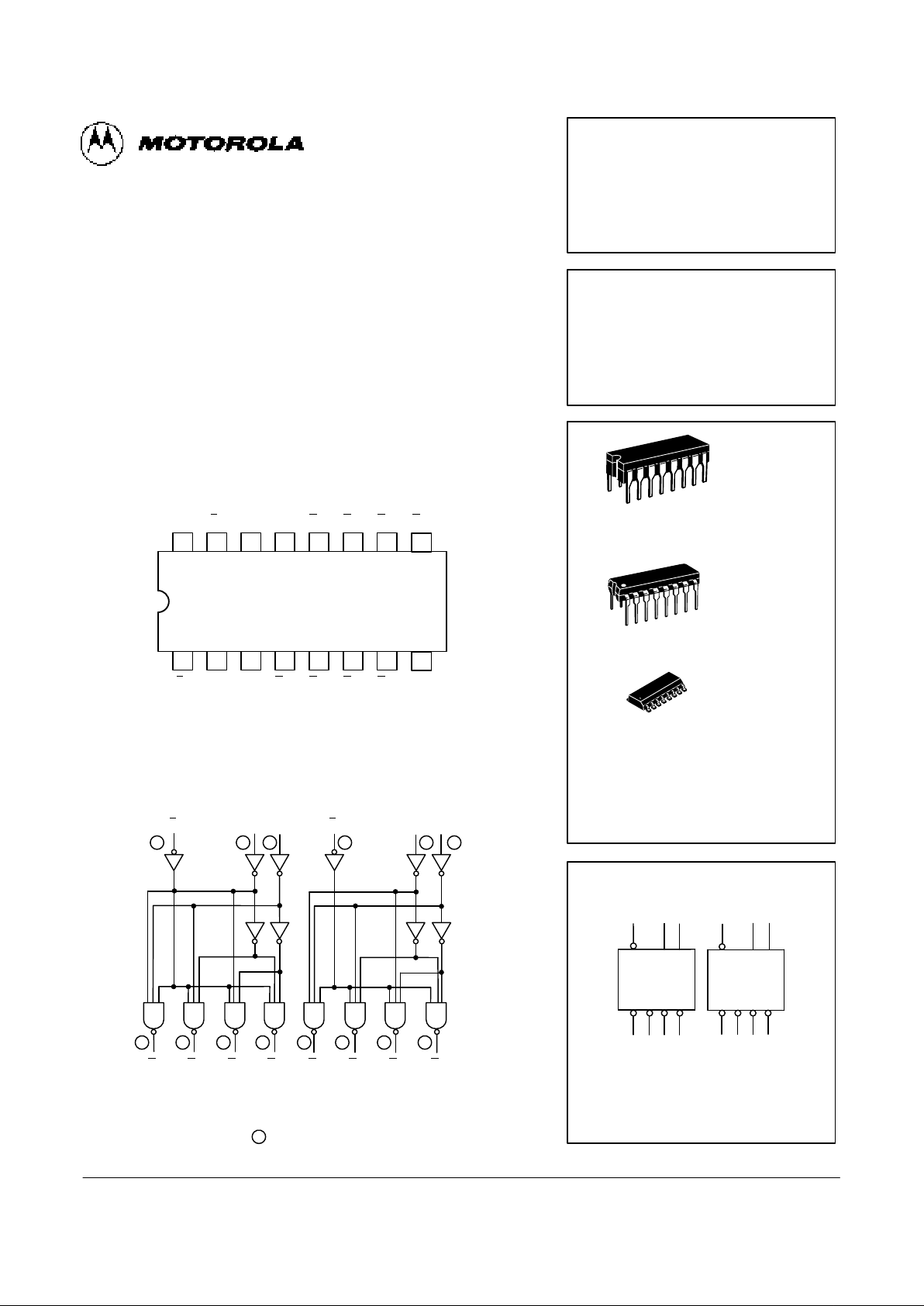
DUAL 1-OF-4 DECODER
The MC54/74F139 is a high speed Dual 1-of-4 Decoder/Demultiplexer.
The device has two independent decoders, each accepting two inputs and
providing four mutually exclusive active LOW outputs. Each decoder has an
active LOW Enable input which can be used as a data input for a 4-output demultiplexer. Each half of the F139 can be used as a function generator providing all four miniterms of two variables.
• Multifunction Capability
• Two Completely Independent 1-of-4 Decoders
• Active Low Mutually Exclusive Outputs
• Input Clamp Diodes Limit High-Speed Termination Effects
CONNECTION DIAGRAM
1516 14 13 12 11 10
21 3 4 5 6 7
V
CC
9
8
E
bA0bA1bO0bO1bO2bO3b
EaA0aA1aO0aO1aO2aO3aGND
VCC = PIN 16
GND = PIN 8
= PIN NUMBERS
91011127654
131415321
LOGIC DIAGRAM
A
1a
A
0a
E
b
O
0b
O
2bO3b
O
3a
O
2a
O
1a
O
0a
O
1b
E
a
A0bA
1b
MC54FXXXJ Ceramic
MC74FXXXN Plastic
MC74FXXXD SOIC
MC54/74F139
DUAL 1-OF-4
DECODER
FAST SHOTTKY TTL
J SUFFIX
CERAMIC
CASE 620-09
N SUFFIX
PLASTIC
CASE 648-08
16
1
16
1
ORDERING INFORMATION
16
1
D SUFFIX
SOIC
CASE 751B-03
LOGIC SYMBOL
VCC = Pin 16
GND = Pin 8
A1A
0
O0O1O2O
3
E A1A
0
O0O1O2O
3
E
1 2 3
4 5 6 7 9101112
131415
4-57
FAST AND LS TTL DATA
MC54/74F139
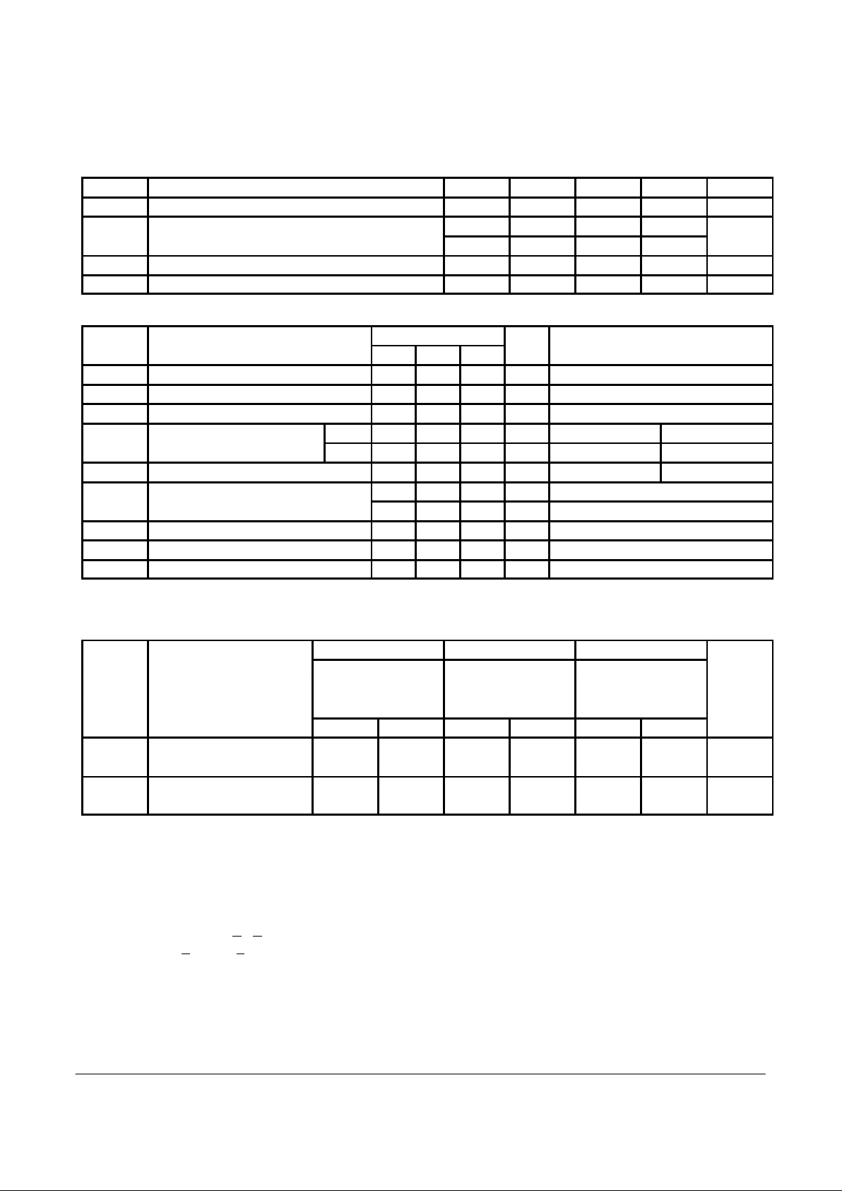
GUARANTEED OPERATING RANGES
Symbol Parameter Min Typ Max Unit
V
CC
Supply Voltage 54, 74 4.5 5.0 5.5 V
T
A
Operating Ambient Temperature Range 54 –55 25 125 °C
74 0 25 70
I
OH
Output Current — High 54, 74 –1.0 mA
I
OL
Output Current — Low 54, 74 20 mA
DC CHARACTERISTICS OVER OPERATING TEMPERATURE RANGE (unless otherwise specified)
Limits
Symbol Parameter Min Typ Max Unit Test Conditions
V
IH
Input HIGH Voltage 2.0 V Guaranteed Input HIGH Voltage
V
IL
Input LOW Voltage 0.8 V Guaranteed Input LOW Voltage
V
IK
Input Clamp Diode Voltage –1.2 V VCC = MIN, IIN = –18 mA
V
OH
Output HIGH Voltage
54, 74 2.5 V IOH = –1.0 mA VCC = 4.50 V
74 2.7 V IOH = –1.0 mA VCC = 4.75 V
V
OL
Output LOW Voltage 0.5 V IOL = 20 mA VCC = MIN
I
IH
Input HIGH Current 20 µA VCC = MAX, VIN = 2.7 V
0.1 mA VCC = MAX, VIN = 7.0 V
I
IL
Input LOW Current –0.6 mA VCC = MAX, VIN = 0.5 V
I
OS
Output Short Circuit Current (Note 2) -60 –150 mA VCC = MAX, V
OUT
= 0 V
I
CC
Power Supply Current 20 mA VCC = MAX
1. For conditions shown as MIN or MAX, use the appropriate value specified under recommended operating conditions for the applicable device type.
2. Not more than one output should be shorted at a time, nor for more than 1 second.
AC CHARACTERISTICS
54/74F 54F 74F
TA = +25°C TA = -55°C to +125°C TA = 0°C to 70°C
VCC = +5.0 V VCC = 5.0 V ±10% VCC = 5.0 V ±10%
CL = 50 pF CL = 50 pF CL = 50 pF
Symbol Parameter Min Max Min Max Min Max Unit
t
PLH
Propagation Delay, 3.5 7.0 2.5 12.0 3.0 8.5 ns
t
PHL
Address to Output 3.5 8.0 3.5 9.5 3.5 9.0
t
PLH
Enable to Output 3.5 7.0 3.0 9.0 3.5 8.0 ns
t
PHL
2.5 6.5 2.5 8.0 2.5 7.5
FUNCTIONAL DESCRIPTION
The F139 is a high speed dual 1-of-4 decoder/demultiplexer
fabricated with the Schottky barrier diode process. The device
has two independent decoders, each of which accepts two
binary weighted inputs (AO, A1) and provide four mutually exclusive active LOW outputs (O
0-O3
). Each decoder has an ac-
tive LOW Enable (E
). When E is HIGH all outputs are forced
HIGH. The enable can be used as the data input for a 4-output
demultiplexer application.
Each half of the F139 generates all four miniterms of two
variables. These four miniterms are useful in some applications, replacing multiple gate functions as shown in Figure 1,
and thereby reducing the number of packages required in a
logic network.
 Loading...