

Motorola MC74ACT823N, MC74AC823DW, MC74AC823N, MC74ACT823DW Datasheet
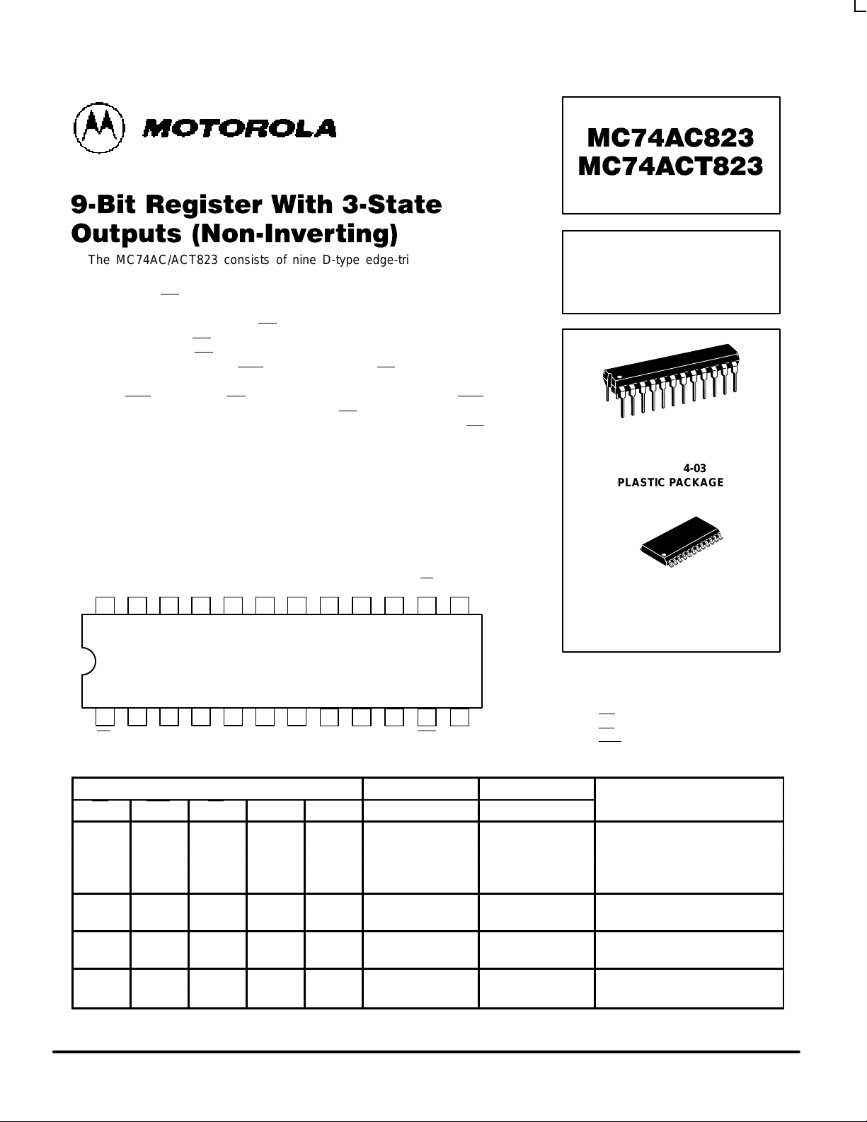
5-1
FACT DATA
Product Preview
" "
"!
The MC74AC/ACT823 consists of nine D-type edge-triggered flip-flops. This
device has 3-state outputs for bus systems, organized in a broadside pinning. In
addition to the clock and output enabled pins, the buffered clock (CP) and buffered
Output Enable (OE
) are common to all flip-flips. The flip-flops will store the state of
their individual D inputs that meet the setup and hold time requirements on the
LOW-to-HIGH CP transition. With OE
LOW, the contents of the flip-flops are available
at the outputs. When OE
is HIGH, the outputs go to the high impedance state.
Operation of the OE
input does not affect the state of the flip-flops. The
MC74AC/ACT823 has Clear (CLR
) and Clock Enable (EN) pins. These devices are
ideal for parity bus interfacing in high performance systems.
When CLR
is LOW, and OE is LOW, the outputs are LOW. When CLR is HIGH,
data can be entered into the flip-flops. When EN
is LOW, data on the inputs is
transferred to the outputs on the LOW-to-HIGH clock transition. When EN
is HIGH,
the outputs do not change state, regardless of the data or clock input transitions.
• 3-State Outputs for Bus Interfacing
• Broad Side Pin Configuration
• ACT has TTL – Compatible Inputs
• High Speed Parallel Positive Edge-Triggered D-Type Flip-Flops
• High Performance Bus Interface Buffering for Busses Carrying Parity
• Outputs Source/Sink 24 mA
Pinout: 24-Lead Packages (Top View)
2324 22 21 20 19 18
V
CC
17
O0O1O2O3O4O5O
6
21 3 4 5 6 7
8
OE
1D0D1D2D3D4D5D6
16
9
O
7
D
7
15
10
O
8
D
8
14
11
EN
CLR
13
12
CP
GND
FUNCTION TABLE
Inputs Internal Outputs
OE CLR EN CP Dn Q O
Operating Mode
H X L ↑ L L Z High Z
H X L ↑ H H Z High Z
H L X X X L Z Clear
L L X X X L L Clear
H H H X X NC Z Hold
L H H X X NC NC Hold
H H L ↑ L L Z Load
H H L ↑ H H Z Load
L H L ↑ L L L Load
L H L ↑ H H H Load
H = HIGH Voltage Level; L = LOW Voltage Level; X = Immaterial; Z = High Impedance State; ↑ = LOW-to-High Transition; NC = No Change
This document contains information on a product under development. Motorola reserves the right to change or discontinue this product without notice.
9-BIT REGISTER WITH
3-STATE OUTPUTS
N SUFFIX
CASE 724-03
PLASTIC PACKAGE
1
24
PIN NAMES
Data Inputs
Data Outputs
Output Enable
Clock Enable
Clear
Clock Input
D0 – D
8
O0 – O
8
OE
EN
CLR
CP
DW SUFFIX
CASE 751E-04
SOIC PACKAGE
MC74AC823 MC74ACT823
5-2
FACT DATA
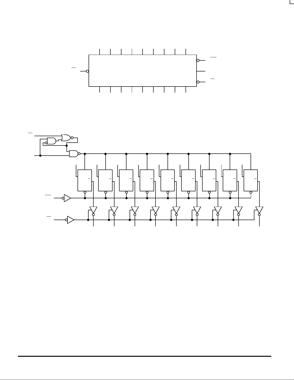
LOGIC SYMBOL
O0O1O2O3O4O5O
6
D0D1D2D3D4D5D
6
O
7
D
7
O
8
D
8
CLR
CP
EN
OE
Q
D
CP
D
0
Q
0
CLR
OE
EN
CP
CLR
Q
D
CP
D
1
Q
1
CLR
Q
D
CP
D
2
Q
2
CLR
Q
D
CP
D
3
Q
3
CLR
Q
D
CP
D
4
Q
4
CLR
Q
D
CP
D
5
Q
5
CLR
Q
D
CP
D
6
Q
6
CLR
Q
D
CP
D
7
Q
7
CLR
Q
D
CP
D
8
Q
8
CLR
LOGIC DIAGRAM
MC74AC823 MC74ACT823
5-3
FACT DATA
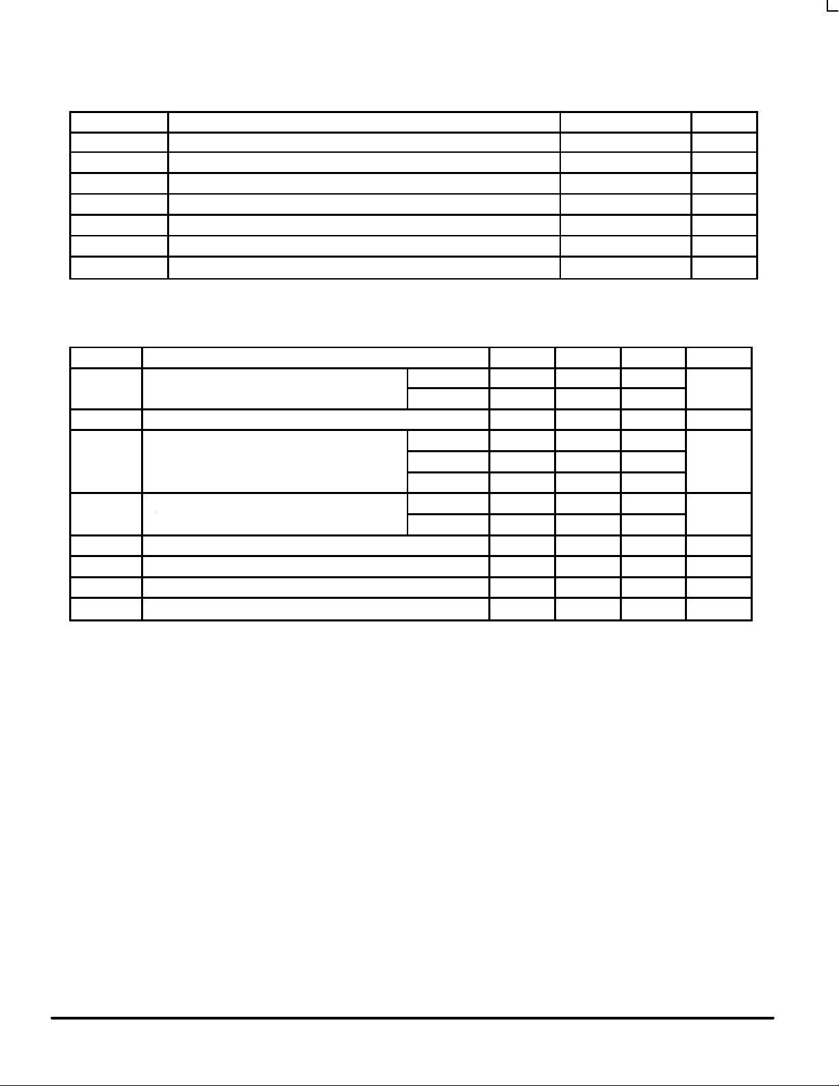
MAXIMUM RATINGS*
Symbol Parameter Value Units
V
CC
DC Supply Voltage (Referenced to GND) –0.5 to +7.0 V
V
in
DC Input Voltage (Referenced to GND) –0.5 to VCC + 0.5 V
V
O
DC Output Voltage (Referenced to GND) –0.5 to VCC + 0.5 V
I
in
DC Input Current, per Pin ± 20 mA
I
out
DC Output Sink/Source Current, per Pin ± 50 mA
I
CC
DC VCC or GND Current per Output Pin ± 50 mA
T
stg
Storage Temperature Range –65 to +150 °C
* Maximum Ratings are those values beyond which damage to the device may occur. Functional operation should be restricted to the Recommended
Operating Conditions.
RECOMMENDED OPERATING CONDITIONS
Symbol Parameter Min Typ Min Unit
′AC 2.0 5.0 6.0
VCCSupply Voltage
′ACT 4.5 5.0 5.5
V
V
in
DC Input Voltage, Output Voltage (Ref. to GND) 0 V
CC
V
VCC @ 3.0 V 150
∆t/∆ v
Input Rise and Fall Time (Note 1)
′AC Devices except Schmitt Inputs
VCC @ 4.5 V 40 ns/V
′AC Devices except Schmitt Inputs
VCC @ 5.5 V 25
VCC @ 4.5 V 10
tr, t
f
Input Rise and Fall Time (Note 2)
′ACT Devices except Schmitt Inputs
VCC @ 5.5 V 8.0
ns/V
T
J
Junction Temperature (PDIP) 140 °C
T
A
Operating Ambient Temperature Range –40 25 85 °C
I
OH
Output Current — HIGH –24 mA
I
OL
Output Current — LOW 24 mA
1. Vin from 30% to 70% VCC; see individual Data Sheets for devices that differ from the typical input rise and fall times.
2. Vin from 0.8 V to 2.0 V; see individual Data Sheets for devices that differ from the typical input rise and fall times.
Input Rise and Fall Time (Note 2)
 Loading...