

Motorola MC74ACT74N, MC74AC74N Datasheet
5-1
FACT DATA
The MC74AC74/74ACT74 is a dual D-type flip-flop with Asynchronous Clear
and Set inputs and complementary (Q,Q
) outputs. Information at the input is
transferred to the outputs on the positive edge of the clock pulse. Clock triggering
occurs at a voltage level of the clock pulse and is not directly related to the transition
time of the positive-going pulse. After the Clock Pulse input threshold voltage has
been passed, the Data input is locked out and information present will not be
transferred to the outputs until the next rising edge of the Clock Pulse input.
Asynchronous Inputs:
LOW input to S
D
(Set) sets Q to HIGH level
LOW input to C
D
(Clear) sets Q to LOW level
Clear and Set are independent of clock
Simultaneous LOW on C
D
and SD makes both Q and Q
HIGH
• Outputs Source/Sink 24 mA
• ′ACT74 Has TTL Compatible Inputs
CP
1
C
D2
CP
2
1314 12 11 10 9 8
21 3 4 5 6 7
V
CC
C
D1D1
CP1SD1Q1Q
1
C
D2D2
CP2SD2Q2Q
2
C
D1
S
D1
Q
1
D
1
S
D2
Q
2
Q
2
D
2
GND
Q
1
PIN NAMES
D1, D
2
Data Inputs
CP1, CP
2
Clock Pulse Inputs
C
D1
, C
D2
Direct Clear Inputs
S
D1
, S
D2
Direct Set Inputs
Q1, Q
1
, Q2, Q2Outputs
TRUTH TABLE (Each Half)
Inputs Outputs
S
D
CDCP D Q Q
L H X X H L
H L X X L H
L L X X H H
H H H H L
H H L L H
H H L X Q
0
Q
0
H = HIGH Voltage Level
L = LOW Voltage Level
X = Immaterial
= LOW-to-HIGH Clock Transition
Q0(Q
0
) = Previous Q(Q
) before
LOW-to-HIGH Transition of Clock
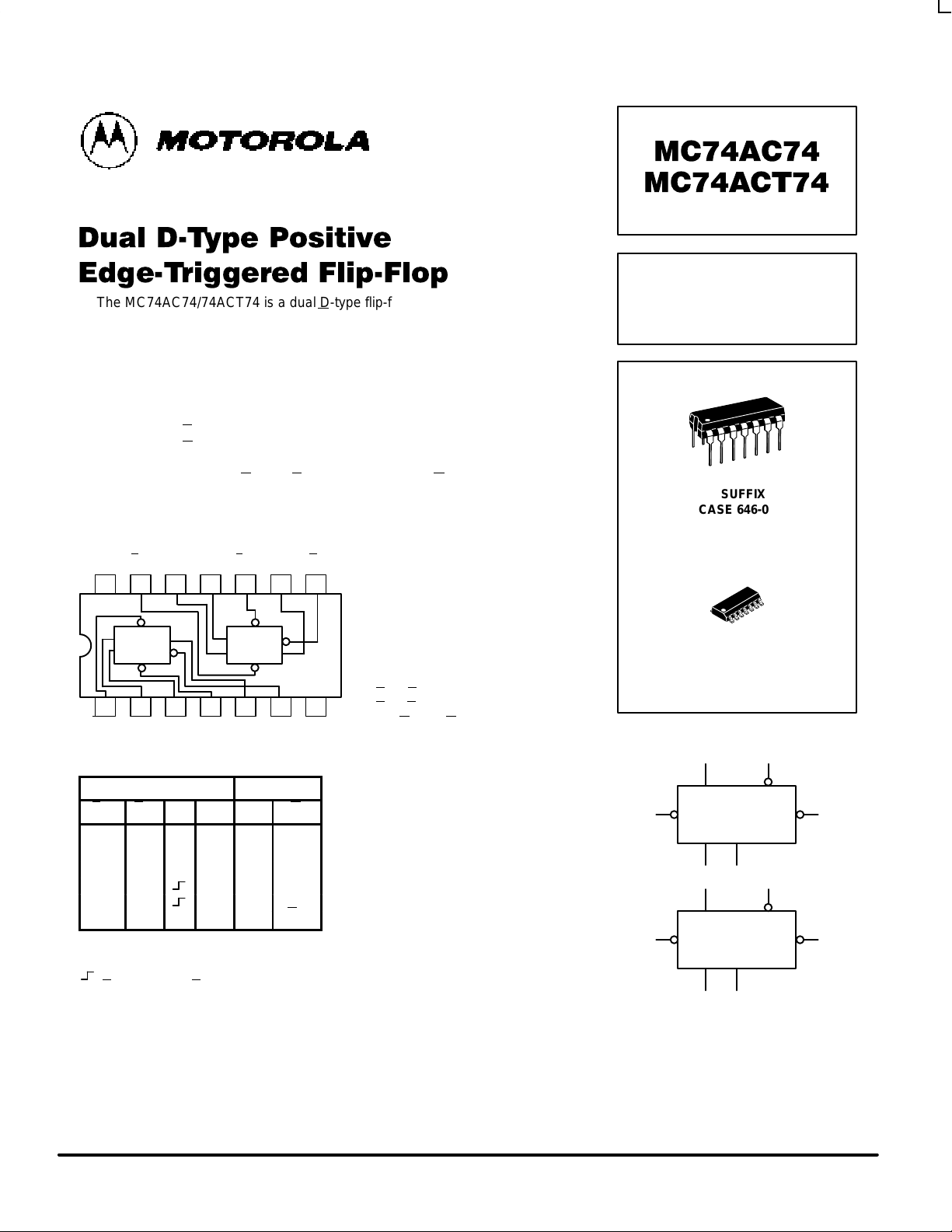
DUAL D-TYPE POSITIVE
EDGE-TRIGGERED
FLIP-FLOP
N SUFFIX
CASE 646-06
PLASTIC
D SUFFIX
CASE 751A-03
PLASTIC
LOGIC SYMBOL
S
D1
Q
1
CP
1
Q
1
C
D1
S
D2
Q
2
D2CP
2
Q
2
CD
2
D
1
MC74AC74 MC74ACT74
5-2
FACT DATA
S
D
D
CP
C
D
Q
Q
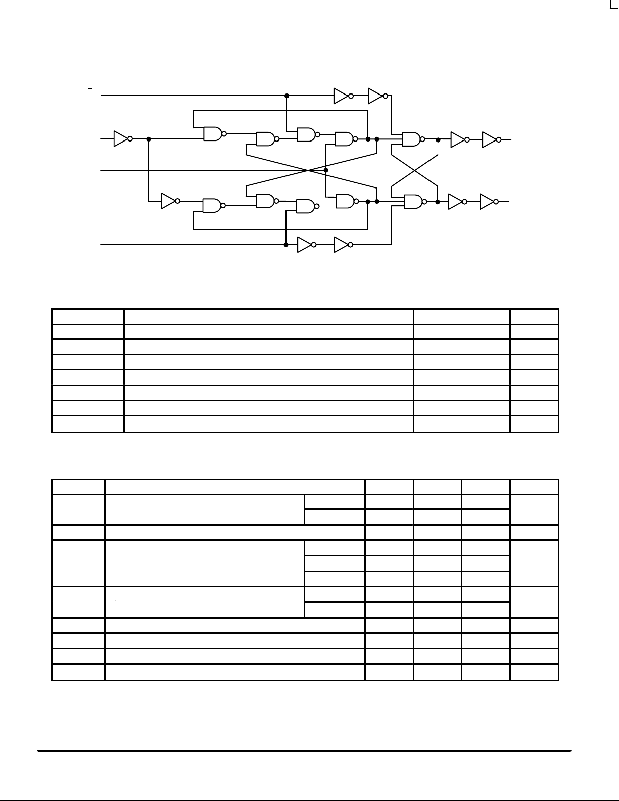
LOGIC DIAGRAM
Please note that this diagram is provided only for the understanding of logic
operations and should not be used to estimate propagation delays.
MAXIMUM RATINGS*
Symbol Parameter Value Unit
V
CC
DC Supply Voltage (Referenced to GND) –0.5 to +7.0 V
V
in
DC Input Voltage (Referenced to GND) –0.5 to VCC +0.5 V
V
out
DC Output Voltage (Referenced to GND) –0.5 to VCC +0.5 V
I
in
DC Input Current, per Pin ±20 mA
I
out
DC Output Sink/Source Current, per Pin ±50 mA
I
CC
DC VCC or GND Current per Output Pin ±50 mA
T
stg
Storage Temperature –65 to +150 °C
* Maximum Ratings are those values beyond which damage to the device may occur. Functional operation should be restricted to the Recommended
Operating Conditions.
RECOMMENDED OPERATING CONDITIONS
Symbol Parameter Min Typ Max Unit
′AC 2.0 5.0 6.0
VCCSupply Voltage
′ACT 4.5 5.0 5.5
V
Vin, V
out
DC Input Voltage, Output Voltage (Ref. to GND) 0 V
CC
V
VCC @ 3.0 V 150
Input Rise and Fall Time (Note 1)
′AC Devices except Schmitt Inputs
VCC @ 4.5 V 40 ns/V
r
, t
f
′AC Devices except Schmitt Inputs
VCC @ 5.5 V 25
VCC @ 4.5 V 10
tr, t
f
Input Rise and Fall Time (Note 2)
′ACT Devices except Schmitt Inputs
VCC @ 5.5 V 8.0
ns/V
T
J
Junction Temperature (PDIP) 140 °C
T
A
Operating Ambient Temperature Range –40 25 85 °C
I
OH
Output Current — High –24 mA
I
OL
Output Current — Low 24 mA
1. Vin from 30% to 70% VCC; see individual Data Sheets for devices that differ from the typical input rise and fall times.
2. Vin from 0.8 V to 2.0 V; see individual Data Sheets for devices that differ from the typical input rise and fall times.
tr, t
f
Input Rise and Fall Time (Note 2)
 Loading...