

5-1
FACT DATA
! # ! !
$!! "!"! $#!
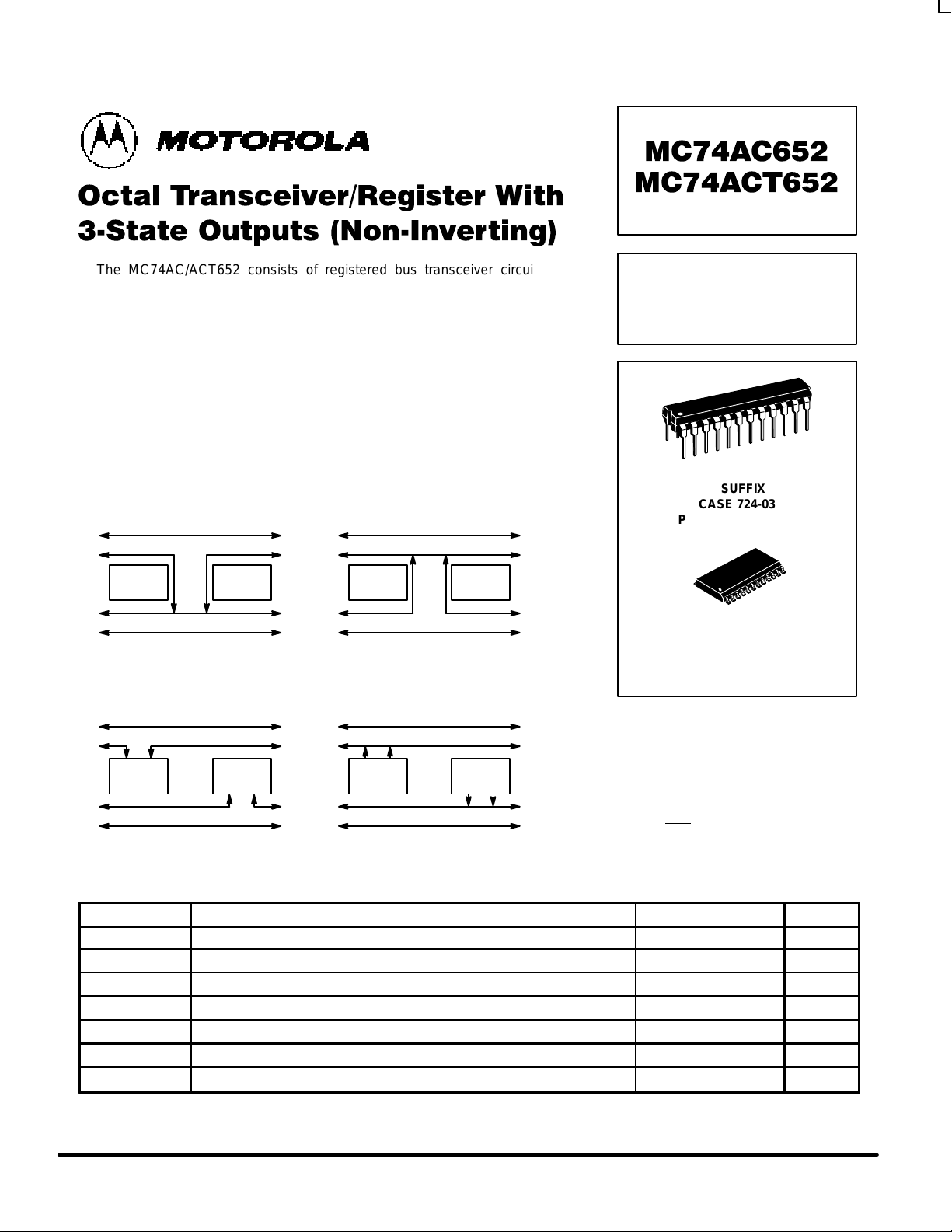
The MC74AC/ACT652 consists of registered bus transceiver circuits, with
outputs, D-type flip-flops and control circuitry providing multiplexed transmission of
data directly from the input bus or from the internal storage registers. Data on the A
or B bus will be loaded into the respective registers on the LOW-to-HIGH transition
of the appropriate clock pin (CAB or CBA). The four fundamental data handling
functions available are illustrated in Figures 1 to 4.
• Independent Registers for A and B Buses
• Multiplexed Real-Time and Stored Data Transfers
• Choice of True and Inverting Data Paths
• 3-State Outputs
• 300 mil Slim Dual-in-Line Package
• Outputs Source/Sink 24 mA
• ′ACT652 Has TTL Compatible Inputs
TRANSFER
FROM REGISTER TO BUS
REG REG
A-BUS
B-BUS
REAL TIME TRANSFER
A-BUS TO B-BUS
REG REG
A-BUS
B-BUS
REAL TIME TRANSFER
B-BUS TO A-BUS
REG REG
A-BUS
B-BUS
Figure 1 Figure 2
STORAGE
FROM BUS TO REGISTER
REG REG
A-BUS
B-BUS
Figure 3 Figure 4
MAXIMUM RATINGS*
Symbol Parameter Value Unit
V
CC
DC Supply Voltage (Referenced to GND) –0.5 to +7.0 V
V
in
DC Input Voltage (Referenced to GND) –0.5 to VCC + 0.5 V
V
out
DC Output Voltage (Referenced to GND) –0.5 to VCC + 0.5 V
I
in
DC Input Current, per Pin ± 20 mA
I
out
DC Output Sink/Source Current, per Pin ± 50 mA
I
CC
DC VCC or GND Current per Output Pin ± 50 mA
T
stg
Storage Temperature –65 to +150 °C
* Maximum Ratings are those values beyond which damage to the device may occur. Functional operation should be restricted to the Recommended
Operating Conditions.
OCTAL TRANSCEIVER/
REGISTER WITH 3-STATE
OUTPUTS (NON-INVERTING)
N SUFFIX
CASE 724-03
PLASTIC PACKAGE
1
24
PIN NAMES
Data Register A Inputs
Data Register A Outputs
Data Register B Inputs
Data Register B Outputs
Clock Pulse Inputs
Transmit/Receive Inputs
Output Enable Inputs
A0 – A
7
B0 – B
7
CAB, CBA
SAB, SBA
GAB, GBA
1
24
DW SUFFIX
CASE 751E-04
SOIC PACKAGE
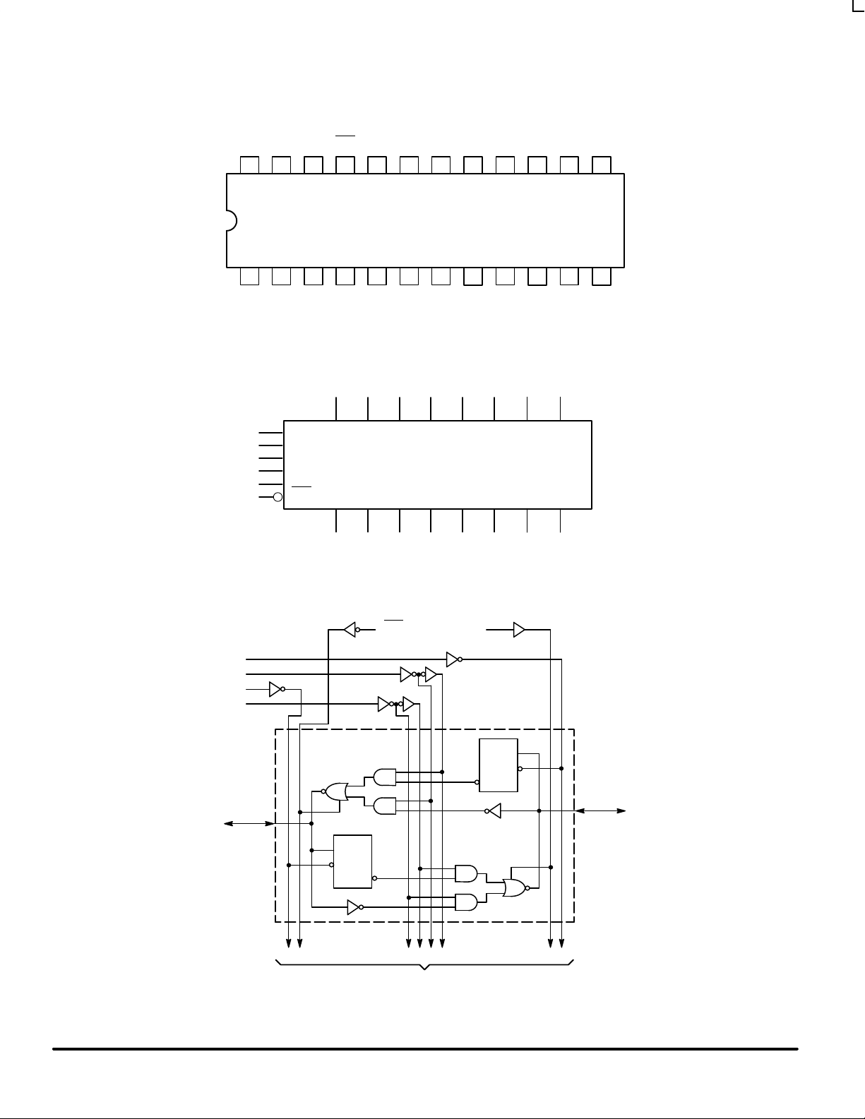
MC74AC652 MC74ACT652
5-2
FACT DATA
Pinout: 24-Lead Plastic Package (Top View)
2324 22 21 20 19 18
21 3 4 5 6 7
V
CC
17
8
16
9
15
10
CBA SBA GBA
B0B1B2B3B4B
5
CAB SAB GAB A0A1A2A3A4A5A
6
14
11
13
12
B6B
7
A7GND
B0B1B2B3B4B
5
A0A1A2A3A4A5A
6
B6B
7
A
7
CAB
SAB
GAB
CBA
SBA
GBA
D
0
C
0
D
0
C
0
CAB
SBA
CBA
SAB
GABGBA
B
0
A
0
1 OF 8 CHANNELS
TO 7 OTHER CHANNELS
Please note that this diagram is provided only for the understanding of logic
operations and should not be used to estimate propagation delays.
LOGIC SYMBOL
LOGIC DIAGRAM
MC74AC652 MC74ACT652
5-3
FACT DATA
FUNCTION TABLE
Inputs Data I/O*
GAB GBA CAB CBA SAB SBA A0 – A
7
B0 – B
7
Operation or Function
L H H or L H or L X X
Isolation
L H ⇑ ⇑ X X
Input
Input
Store A and B Data
X H ⇑ H or L X X Input Unspecified* Store A, Hold B
H H ⇑ ⇑ X** X Input Output Store A in Both Registers
L X H or L ⇑ X X Unspecified* Input Hold A, Store B
L L ⇑ ⇑ X X** Output Input Store B in Both Registers
L L X X X L
Real-Time B Data to A Bus
L L X H or L X H
Output
Input
Stored B Data to A Bus
H H X X L X
Real-Time A Data to B Bus
H H H or L X H X
Input
Output
Stored A Data to B Bus
Stored A Data to B Bus and
HLH or L
H or LHH
Output
Output
Stored A Data to B Bus and
Stored B Data to A Bus
* The data output functions may be enabled or disabled by various signals at the GBA and GAB inputs. Data input functions are always enabled; i.e., data at the
bus pins will be stored on every LOW-to-HIGH transition of the appropriate clock inputs.
** Select control = L: clocks can occur simultaneously.
H = HIGH Voltage Level; L = LOW Voltage Level; X = Immaterial; ⇑ = LOW-to-HIGH Transition
RECOMMENDED OPERATING CONDITIONS
Symbol Parameter Min Typ Min Unit
′AC 2.0 5.0 6.0
VCCSupply Voltage
′ACT 4.5 5.0 5.5
V
Vin, V
out
DC Input Voltage, Output Voltage (Ref. to GND) 0 V
CC
V
VCC @ 3.0 V 150
Input Rise and Fall Time (Note 1)
′AC Devices except Schmitt Inputs
VCC @ 4.5 V 40 ns/V
r
, t
f
′AC Devices except Schmitt Inputs
VCC @ 5.5 V 25
VCC @ 4.5 V 10
tr, t
f
Input Rise and Fall Time (Note 2)
′ACT Devices except Schmitt Inputs
VCC @ 5.5 V 8.0
ns/V
T
J
Junction Temperature (PDIP) 140 °C
T
A
Operating Ambient Temperature Range –40 25 85 °C
I
OH
Output Current — HIGH –24 mA
I
OL
Output Current — LOW 24 mA
1. Vin from 30% to 70% VCC; see individual Data Sheets for devices that differ from the typical input rise and fall times.
2. Vin from 0.8 V to 2.0 V; see individual Data Sheets for devices that differ from the typical input rise and fall times.
tr, t
f
Input Rise and Fall Time (Note 2)
 Loading...