

Motorola MC74ACT648DW, MC74ACT648N, MC74AC648N Datasheet
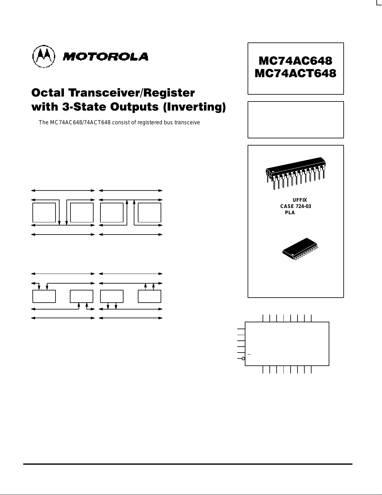
5-1
FACT DATA
Product Preview
!
The MC74AC648/74ACT648 consist of registered bus transceiver circuits,
with outputs, D-type flip-flops and control circuitry providing multiplexed transmission
of data directly from the input bus or from the internal storage registers. Data on the
A or B bus will be loaded into the respective registers on the LOW-to-HIGH transition
of the appropriate clock pin (CAB or CBA). The four fundamental data handling
functions available are illustrated in the following figures.
REAL TIME TRANSFER
A-BUS TO B-BUS
REAL TIME TRANSFER
B-BUS TO A-BUS
REG
REG REG REG
REG REG REG REG
B-BUS B-BUS
A-BUS A-BUS
B-BUS B-BUS
A-BUS A-BUS
STORAGE
FROM BUS TO REGISTER
TRANSFER
FROM REGISTER TO BUS
Figure 1 Figure 2
Figure 3 Figure 4
• Independent Registers for A and B Buses
• Multiplexed Real-Time and Stored Data Transfers
• Choice of True and Inverting Data Paths
• 3-State Outputs
• 300 mil Slim Dual In-Line Package
• Outputs Source/Sink 24 mA
This document contains information on a product under development. Motorola reserves the right to change or discontinue this product without notice.
OCTAL
TRANSCEIVER/REGISTER
WITH 3-STATE OUTPUTS
(INVERTING)
N SUFFIX
CASE 724-03
PLASTIC
DW SUFFIX
CASE 751E-04
SOIC PACKAGE
LOGIC SYMBOL
A0A1A2A3A4A5A6A
7
B0B1B2B3B4B5B6B
7
CAB
SAB
DIR
CBA
SBA
G
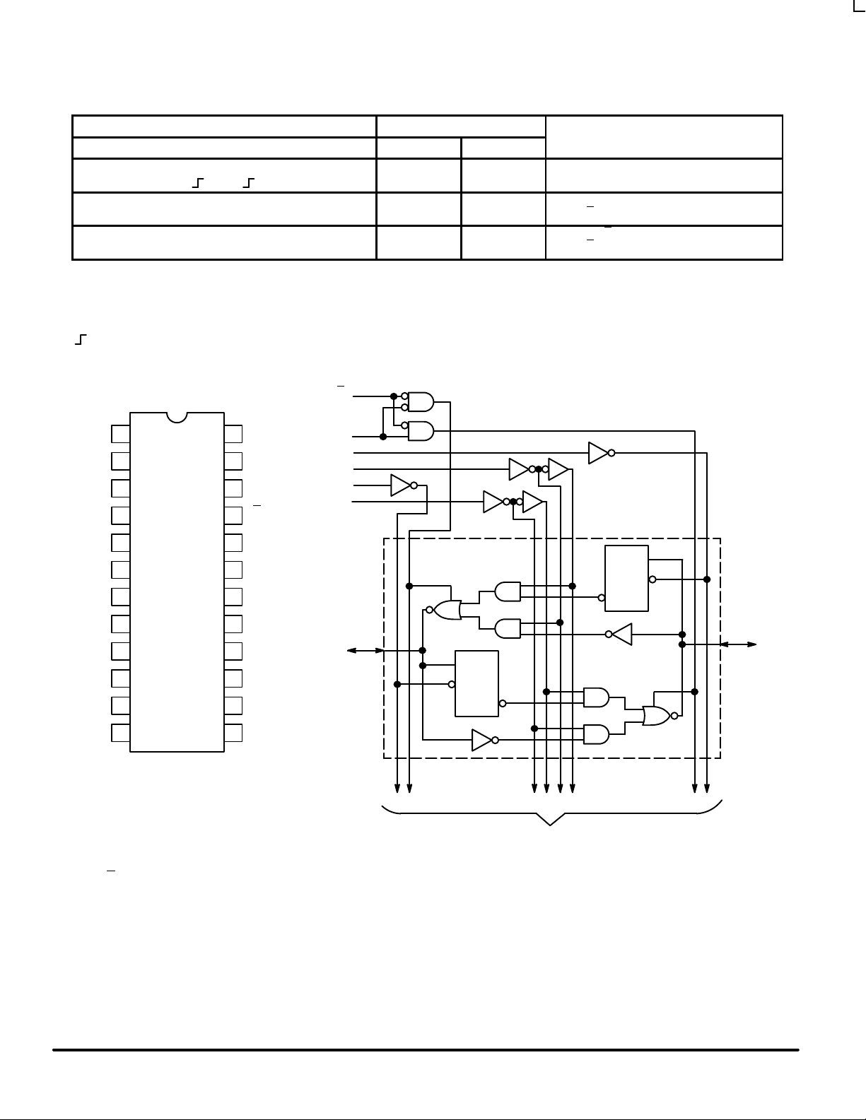
MC74AC648 MC74ACT648
5-2
FACT DATA
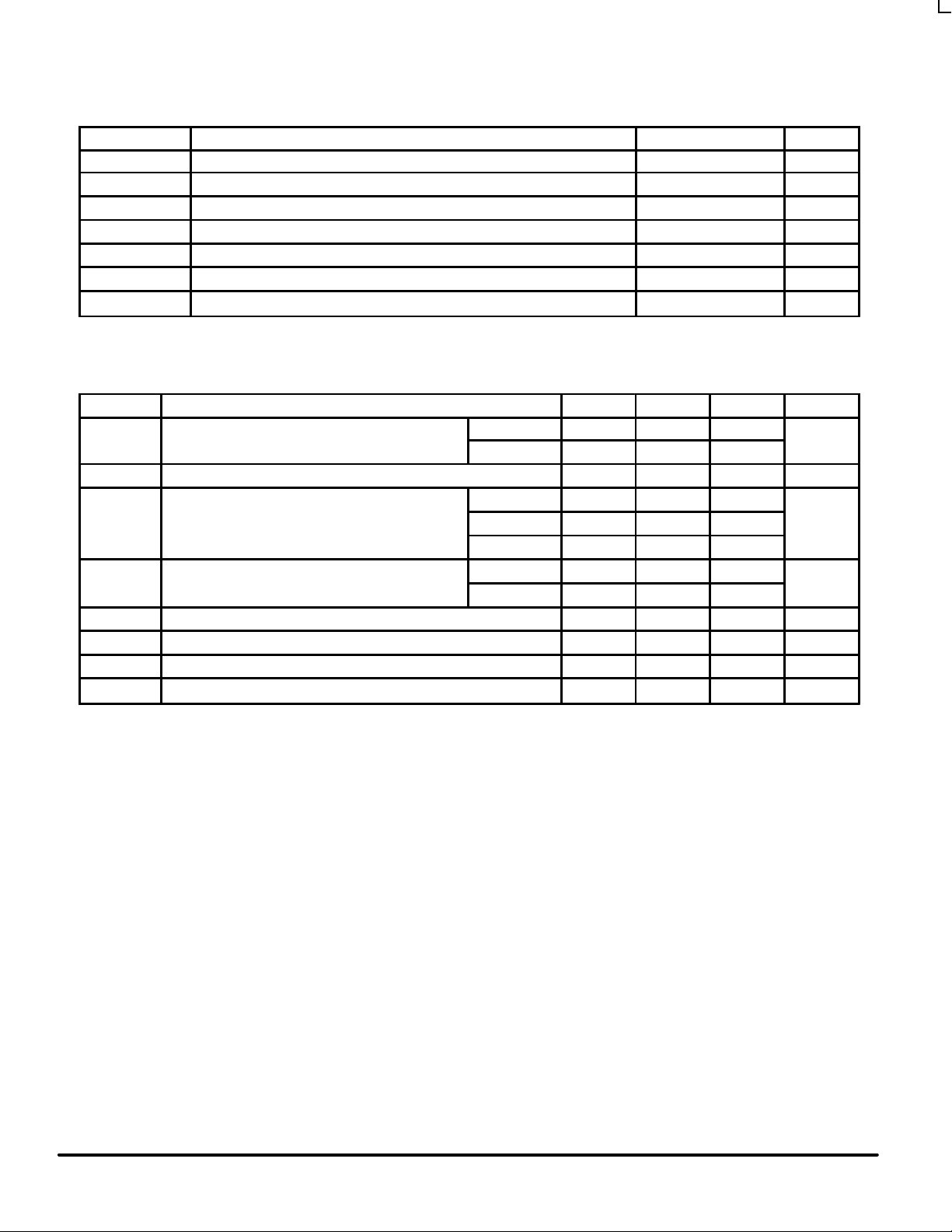
FUNCTION TABLE
Inputs Data I/O*
G DIR CAB CBA SAB SBA A0–A
7
B0–B
7
Operation or Function
H
H
X
X
H or L H or L X
X
X
X
Input Input
Isolation
Store A and B Data
L
L
L
L
X
X
X
X
X
X
L
H
Output Input
Real Time B Data to A Bus
Stored B
Data to A Bus
L
L
H
H
X
H or L
X
X
L
H
X
X
Input Output
Real Time A Data to B Bus
Stored A
Data to B Bus
* The data output functions may be enabled or disabled by various signals at the G and DIR inputs. Data input functions are always enabled; i.e., data at the bus
pins will be stored on every LOW-to-HIGH transition of the appropriate clock inputs.
H = HIGH Voltage Level
L = LOW Voltage Level
X = Immaterial
= LOW-to-HIGH Transition
1 OF 8 CHANNELS
D
0
C
0
D
0
C
0
CAB
SAB
DIR
CBA
SBA
G
B
0
A
0
TO 7 OTHER CHANNELS
LOGIC DIAGRAM
Please note that this diagram is provided only for the understanding of logic
operations and should not be used to estimate propagation delays.
1
CAB
2
SAB
3
DIR
4
A
0
5
A
1
6
A
2
7
A
3
8
A
4
9
A
5
10
A
6
11
A
7
12
GND
24
23
22
21
20
19
18
17
16
14
13
V
CC
CBA
SBA
G
B
0
B
1
B
2
B
3
B
4
B
5
B
6
B
7
PIN NAMES
A0–A7 Data Register Inputs
Data Register A Outputs
B0–B
7
Data Register B Inputs
Data Register B Outputs
CAB, CBA Clock Pulse Inputs
SAB, SBA Transmit/Receive Inputs
DIR, G
Output Enable Inputs
15
MC74AC648 MC74ACT648
5-3
FACT DATA
MAXIMUM RATINGS*
Symbol Parameter Value Unit
V
CC
DC Supply Voltage (Referenced to GND) –0.5 to +7.0 V
V
in
DC Input Voltage (Referenced to GND) –0.5 to VCC +0.5 V
V
out
DC Output Voltage (Referenced to GND) –0.5 to VCC +0.5 V
I
in
DC Input Current, per Pin ±20 mA
I
out
DC Output Sink/Source Current, per Pin ±50 mA
I
CC
DC VCC or GND Current per Output Pin ±50 mA
T
stg
Storage Temperature –65 to +150 °C
* Maximum Ratings are those values beyond which damage to the device may occur. Functional operation should be restricted to the Recommended
Operating Conditions.
RECOMMENDED OPERATING CONDITIONS
Symbol Parameter Min Typ Max Unit
′AC 2.0 5.0 6.0
VCCSupply Voltage
′ACT 4.5 5.0 5.5
V
Vin, V
out
DC Input Voltage, Output Voltage (Ref. to GND) 0 V
CC
V
VCC @ 3.0 V 150
Input Rise and Fall Time (Note 1)
′AC Devices except Schmitt Inputs
VCC @ 4.5 V 40 ns/V
r
, t
f
′AC Devices except Schmitt Inputs
VCC @ 5.5 V 25
VCC @ 4.5 V 10
tr, t
f
Input Rise and Fall Time (Note 2)
′ACT Devices except Schmitt Inputs
VCC @ 5.5 V 8.0
ns/V
T
J
Junction Temperature (PDIP) 140 °C
T
A
Operating Ambient Temperature Range –40 25 85 °C
I
OH
Output Current — High –24 mA
I
OL
Output Current — Low 24 mA
1. Vin from 30% to 70% VCC; see individual Data Sheets for devices that differ from the typical input rise and fall times.
2. Vin from 0.8 V to 2.0 V; see individual Data Sheets for devices that differ from the typical input rise and fall times.
tr, t
f
Input Rise and Fall Time (Note 2)
 Loading...