

Motorola MC74ACT564DW, MC74ACT564DWR2, MC74ACT564N, MC74AC564DW, MC74AC564N Datasheet
5-1
FACT DATA
The MC74AC564/74ACT564 is a high-speed, low power octal flip-flop with
a buffered common Clock (CP) and a buffered common Output Enable (OE
).
The information presented to the D inputs is stored in the flip-flops on the LOW-toHIGH Clock (CP) transition.
The MC74AC564/74ACT564 device is functionally identical to the MC74AC574/
74ACT574, but with inverted outputs.
• Inputs and Outputs on Opposite Sides of Package Allowing Easy Interface with
Microprocessors
• Useful as Input or Output Port for Microprocessors
• Functionally Identical to MC74AC574/74ACT574 but with Inverted Outputs
• 3-State Outputs for Bus-Oriented Applications
• Outputs Source/Sink 24 mA
• ′ACT564 Has TTL Compatible Inputs
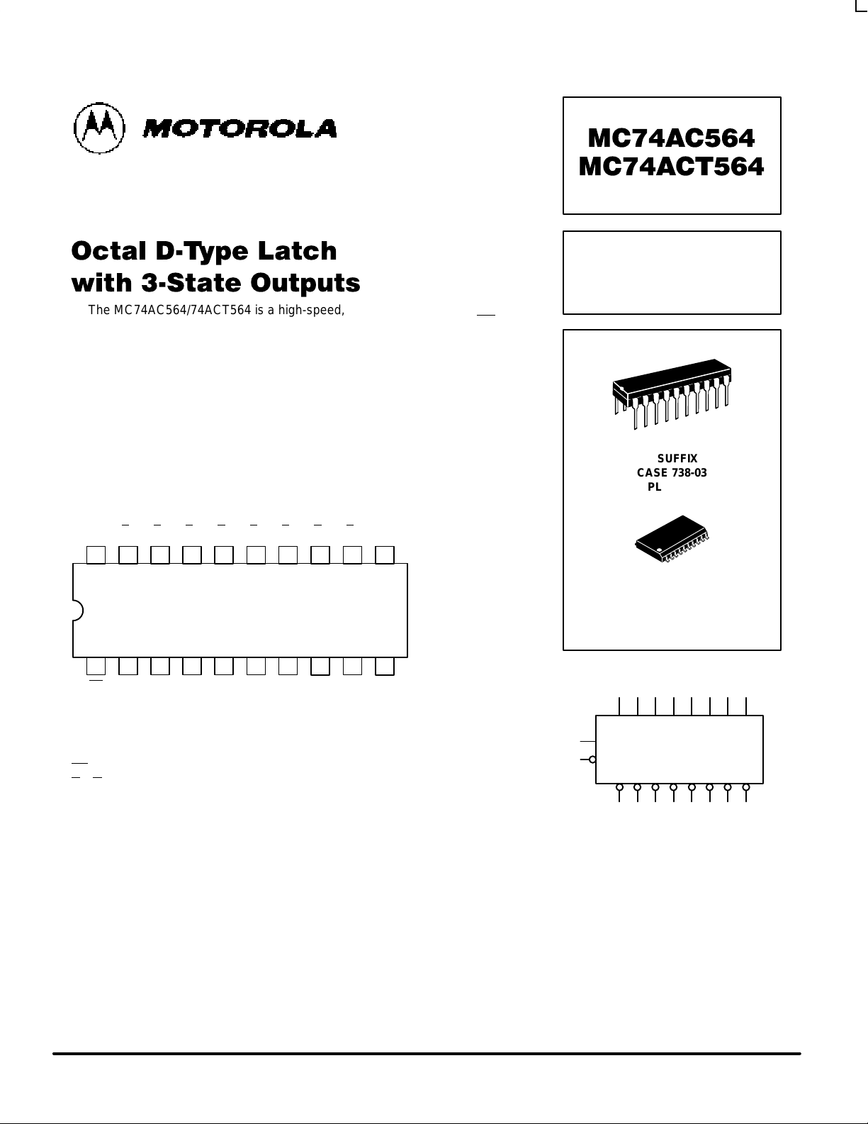
1920 18 17 16 15 14
21 3 4 5 6 7
V
CC
13
8
12
9
11
10
O0O1O2O3O4O5O6O7CP
OE
D0D1D2D3D4D5D6D7GND
PIN NAMES
D0–D7 Data Inputs
CP Clock Pulse Input
OE
3-State Output Enable Input
O
0–O7
3-State Outputs
OCTAL D-TYPE
LATCH WITH
3-STATE OUTPUTS
N SUFFIX
CASE 738-03
PLASTIC
DW SUFFIX
CASE 751D-04
PLASTIC
LOGIC SYMBOL
O0O1O2O3O4O5O6O
7
D0D1D2D3D4D5D6D
7
CP
OE
MC74AC564 MC74ACT564
5-2
FACT DATA
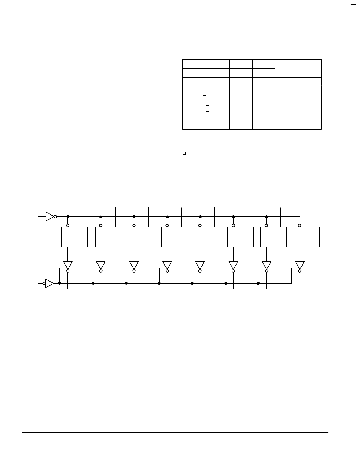
FUNCTIONAL DESCRIPTION
The MC74AC564/74ACT564 consists of eight edgetriggered flip-flops with individual D-type inputs and 3-state
complementary outputs. The buffered clock and buffered
Output Enable are common to all flip-flops. The eight flip-flops
will store the state of their individual D inputs that meet the
setup and hold times requirements on the LOW-to-HIGH
Clock (CP) transition. With the Output Enable (OE
) LOW, the
contents of the eight flip-flops are available at the outputs.
When OE
is HIGH, the outputs go to the high impedance state.
Operation of the OE
input does not affect the state of the
flip-flops.
FUNCTION TABLE
Inputs Internal Outputs
OE CP D Q O
Function
H H L NC Z Hold
H H H NC Z Hold
H L H Z Load
H H L Z Load
L L H H Data Available
L H L L Data Available
L H L NC NC No Change in Data
L H H NC NC No Change in Data
H = HIGH Voltage Level
L = LOW Voltage Level
X = Immaterial
Z = High Impedance
= LOW-to-HIGH Transition
NC = No Change
LOGIC DIAGRAM
D
0
D
1
D
2
D
3
D
4
D
5
D
6
D
7
C D
Q
O
0
O
1
O
2
O
3
O
4
O
5
O
6
O
7
OE
CP
C D
Q
C D
Q
C D
Q
C D
Q
C D
Q
C D
Q
C D
Q
Please note that this diagram is provided only for the understanding of logic
operations and should not be used to estimate propagation delays.
MC74AC564 MC74ACT564
5-3
FACT DATA
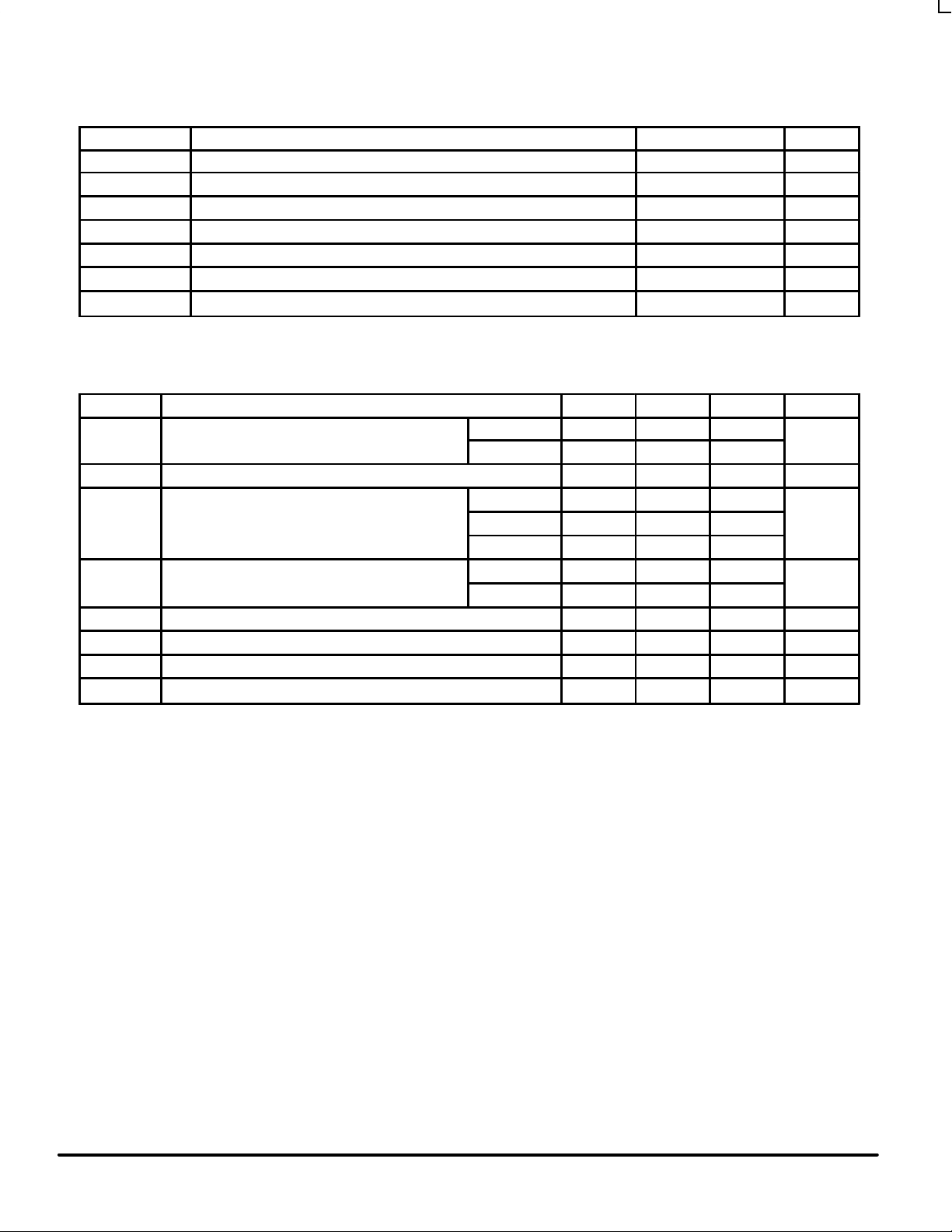
MAXIMUM RATINGS*
Symbol Parameter Value Unit
V
CC
DC Supply Voltage (Referenced to GND) –0.5 to +7.0 V
V
in
DC Input Voltage (Referenced to GND) –0.5 to VCC +0.5 V
V
out
DC Output Voltage (Referenced to GND) –0.5 to VCC +0.5 V
I
in
DC Input Current, per Pin ±20 mA
I
out
DC Output Sink/Source Current, per Pin ±50 mA
I
CC
DC VCC or GND Current per Output Pin ±50 mA
T
stg
Storage Temperature –65 to +150 °C
* Maximum Ratings are those values beyond which damage to the device may occur. Functional operation should be restricted to the Recommended
Operating Conditions.
RECOMMENDED OPERATING CONDITIONS
Symbol Parameter Min Typ Max Unit
′AC 2.0 5.0 6.0
VCCSupply Voltage
′ACT 4.5 5.0 5.5
V
Vin, V
out
DC Input Voltage, Output Voltage (Ref. to GND) 0 V
CC
V
VCC @ 3.0 V 150
Input Rise and Fall Time (Note 1)
′AC Devices except Schmitt Inputs
VCC @ 4.5 V 40 ns/V
r
, t
f
′AC Devices except Schmitt Inputs
VCC @ 5.5 V 25
VCC @ 4.5 V 10
tr, t
f
Input Rise and Fall Time (Note 2)
′ACT Devices except Schmitt Inputs
VCC @ 5.5 V 8.0
ns/V
T
J
Junction Temperature (PDIP) 140 °C
T
A
Operating Ambient Temperature Range –40 25 85 °C
I
OH
Output Current — High –24 mA
I
OL
Output Current — Low 24 mA
1. Vin from 30% to 70% VCC; see individual Data Sheets for devices that differ from the typical input rise and fall times.
2. Vin from 0.8 V to 2.0 V; see individual Data Sheets for devices that differ from the typical input rise and fall times.
tr, t
f
Input Rise and Fall Time (Note 2)
 Loading...