

Motorola MC74ACT540DW, MC74ACT541N, MC74ACT541DW, MC74ACT540N, MC74AC540DW Datasheet
...
5-1
FACT DATA
!
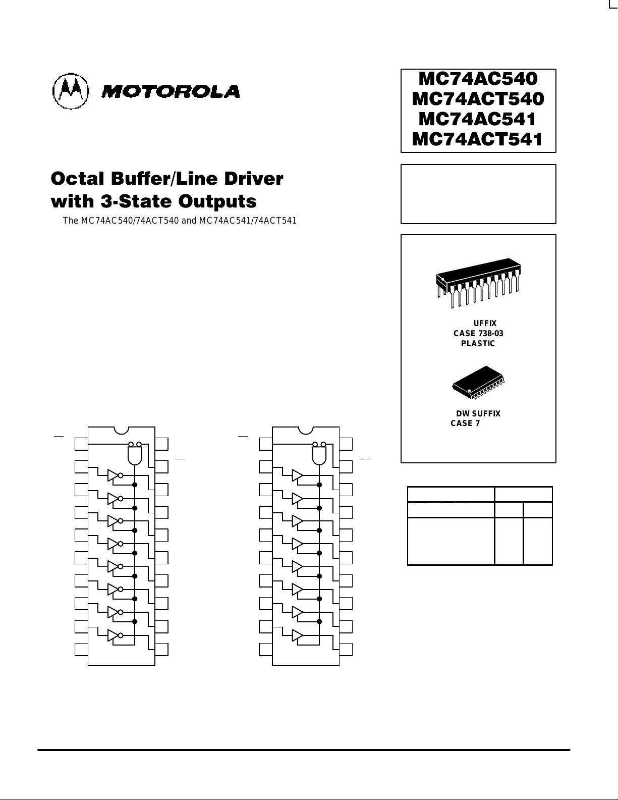
The MC74AC540/74ACT540 and MC74AC541/74ACT541 are octal buffer/line
drivers designed to be employed as memory and address drivers, clock drivers and
bus oriented transmitter/receivers. The MC74AC541/74ACT541 is a noninverting
option of the MC74AC540/74ACT540.
These devices are similar in function to the MC74AC240/74ACT240 and
MC74AC244/74ACT244 while providing flow-through architecture (inputs on opposite
side from outputs). This pinout arrangement makes these devices especially useful
as output ports for microprocessors, allowing ease of layout and greater PC board
density.
• 3-State Outputs
• Inputs and Outputs Opposite Side of Package, Allowing
Easier Interface to Microprocessors
• Outputs Source/Sink 24 mA
• MC74AC540/74ACT540 Provides Inverted Outputs
• MC74AC541/74ACT541 Provides Noninverted Outputs
• ′ACT540 and ′ACT541 Have TTL Compatible Inputs
TRUTH TABLE
Inputs Outputs
OE1OE
2
D ′540 ′541
L L H L H
H X X Z Z
X H X Z Z
L L L H L
H = HIGH Voltage Level
L = LOW Voltage Level
X = Immaterial
Z = High Impedance
OCTAL
BUFFER/LINE DRIVER
WITH 3-STATE
OUTPUTS
N SUFFIX
CASE 738-03
PLASTIC
DW SUFFIX
CASE 751D-04
PLASTIC
1
OE
1
2
3
4
5
6
7
8
9
10
GND
20
19
18
17
16
15
14
13
12
11
V
CC
OE
2
MC74AC540/74ACT540
1
OE
1
2
3
4
5
6
7
8
9
10
GND
20
19
18
17
16
15
14
13
12
11
V
CC
OE
2
MC74AC541/74ACT541
MC74AC540 MC74ACT540 MC74AC541 MC74ACT541
5-2
FACT DATA
MAXIMUM RATINGS*
Symbol Parameter Value Unit
V
CC
DC Supply Voltage (Referenced to GND) –0.5 to +7.0 V
V
in
DC Input Voltage (Referenced to GND) –0.5 to VCC +0.5 V
V
out
DC Output Voltage (Referenced to GND) –0.5 to VCC +0.5 V
I
in
DC Input Current, per Pin ±20 mA
I
out
DC Output Sink/Source Current, per Pin ±50 mA
I
CC
DC VCC or GND Current per Output Pin ±50 mA
T
stg
Storage Temperature –65 to +150 °C
* Maximum Ratings are those values beyond which damage to the device may occur. Functional operation should be restricted to the Recommended
Operating Conditions.
RECOMMENDED OPERATING CONDITIONS
Symbol Parameter Min Typ Max Unit
′AC 2.0 5.0 6.0
VCCSupply Voltage
′ACT 4.5 5.0 5.5
V
Vin, V
out
DC Input Voltage, Output Voltage (Ref. to GND) 0 V
CC
V
VCC @ 3.0 V 150
Input Rise and Fall Time (Note 1)
′AC Devices except Schmitt Inputs
VCC @ 4.5 V 40 ns/V
r
, t
f
′AC Devices except Schmitt Inputs
VCC @ 5.5 V 25
VCC @ 4.5 V 10
tr, t
f
Input Rise and Fall Time (Note 2)
′ACT Devices except Schmitt Inputs
VCC @ 5.5 V 8.0
ns/V
T
J
Junction Temperature (PDIP) 140 °C
T
A
Operating Ambient Temperature Range –40 25 85 °C
I
OH
Output Current — High –24 mA
I
OL
Output Current — Low 24 mA
1. Vin from 30% to 70% VCC; see individual Data Sheets for devices that differ from the typical input rise and fall times.
2. Vin from 0.8 V to 2.0 V; see individual Data Sheets for devices that differ from the typical input rise and fall times.
tr, t
f
Input Rise and Fall Time (Note 2)
MC74AC540 MC74ACT540 MC74AC541 MC74ACT541
5-3
FACT DATA
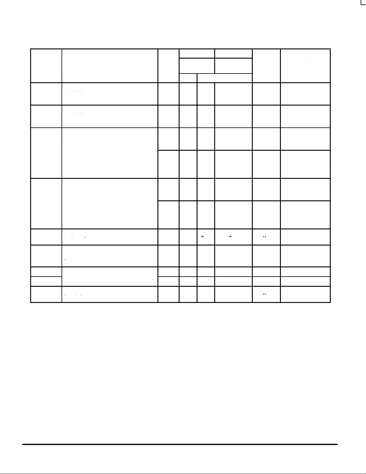
DC CHARACTERISTICS
74AC 74AC
Symbol
Parameter
V
CC
(V)
TA = +25°C
TA =
–40°C to +85°C
Unit
Conditions
Typ Guaranteed Limits
V
IH
3.0 1.5 2.1 2.1 V
OUT
= 0.1 V
4.5 2.25 3.15 3.15 V or VCC – 0.1 V
5.5 2.75 3.85 3.85
V
IL
3.0 1.5 0.9 0.9 V
OUT
= 0.1 V
4.5 2.25 1.35 1.35 V or VCC – 0.1 V
5.5 2.75 1.65 1.65
V
OH
3.0 2.99 2.9 2.9 I
OUT
= –50 µA
4.5 4.49 4.4 4.4 V
5.5 5.49 5.4 5.4
*VIN = VIL or V
IH
3.0 2.56 2.46
–12 mA
4.5 3.86 3.76
V
I
OH
–24 mA
5.5 4.86 4.76 –24 mA
V
OL
3.0 0.002 0.1 0.1 I
OUT
= 50 µA
4.5 0.001 0.1 0.1 V
5.5 0.001 0.1 0.1
*VIN = VIL or V
IH
3.0 0.36 0.44
12 mA
4.5 0.36 0.44
V
I
OL
24 mA
5.5 0.36 0.44 24 mA
I
IN
5.5
±0.1
±1.0
µA
VI = VCC, GND
I
OZ
VI (OE) = VIL, V
IH
5.5 ±0.5 ±5.0 µA VI = VCC, GND
VO = VCC, GND
I
OLD
5.5 75 mA V
OLD
= 1.65 V Max
I
OHD
Output Current
5.5 –75 mA V
OHD
= 3.85 V Min
I
CC
5.5
8.080µA
VIN = VCC or GND
* All outputs loaded; thresholds on input associated with output under test.
†Maximum test duration 2.0 ms, one output loaded at a time.
Note: IIN and ICC @ 3.0 V are guaranteed to be less than or equal to the respective limit @ 5.5 V VCC.
Minimum High Level
Input Voltage
Maximum Low Level
Input Voltage
Minimum High Level
Output Voltage
Maximum Low Level
Output Voltage
Maximum Input
Leakage Current
Maximum
3-State
Current
†Minimum Dynamic
Maximum Quiescent
Supply Current
 Loading...