

Motorola MC74ACT373DW, MC74AC373N, MC74AC373DW Datasheet
5-1
FACT DATA
The MC74AC373/74ACT373 consists of eight latches with 3-state outputs for bus
organized system applications. The flip-flops appear transparent to the data when
Latch Enable (LE) is HIGH. When LE is LOW, the data that meets the setup time is
latched. Data appears on the bus when the Output Enable (OE
) is LOW. When OE
is HIGH, the bus output is in the high impedance state.
• Eight Latches in a Single Package
• 3-State Outputs for Bus Interfacing
• Outputs Source/Sink 24 mA
• ′ACT373 Has TTL Compatible Inputs
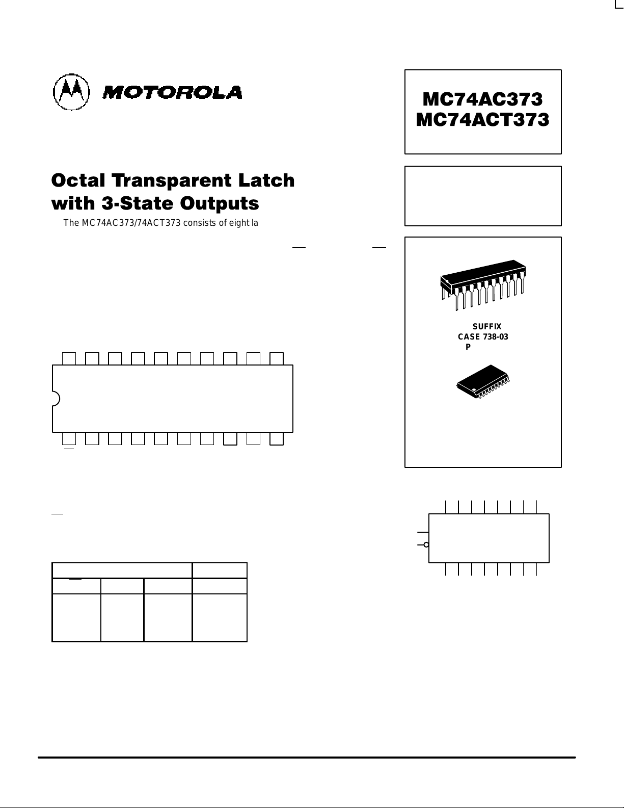
1920 18 17 16 15 14
21 3 4 5 6 7
V
CC
13
8
12
9
11
10
O7D7D6O6O5D5D4O4LE
OE
O0D0D1O1O2D2D3O3GND
PIN NAMES
D0–D7 Data Inputs
LE Latch Enable Input
OE
Output Enable Input
O0–O73-State Latch Outputs
TRUTH TABLE
Inputs Outputs
OE LE D
n
O
n
H X X Z
L H L L
L H H H
L L X O
0
H = HIGH Voltage Level
L = LOW Voltage Level
Z = High Impedance
X = Immaterial
O0 = Previous O0 before LOW-to-HIGH Transition of Clock
OCTAL TRANSPARENT
LATCH WITH
3-STATE OUTPUTS
N SUFFIX
CASE 738-03
PLASTIC
DW SUFFIX
CASE 751D-04
PLASTIC
LOGIC SYMBOL
O0O1O2O3O4O5O6O
7
D0D1D2D3D4D5D6D
7
LE
OE
MC74AC373 MC74ACT373
5-2
FACT DATA
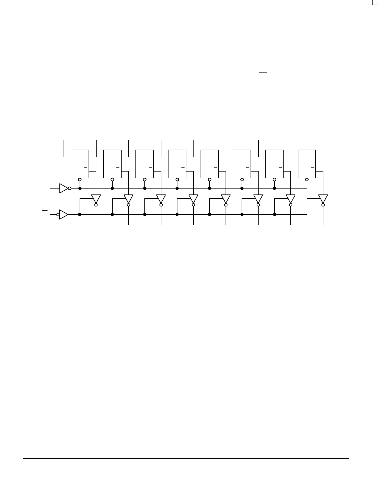
FUNCTIONAL DESCRIPTION
The MC74AC373/74ACT373 contains eight D-type latches
with 3-state standard outputs. When the Latch Enable (LE)
input is HIGH, data on the Dn inputs enters the latches. In this
condition the latches are transparent, i.e., a latch output will
change state each time its D input changes. When LE is LOW,
the latches store the information that was present on the D
inputs a setup time preceding the HIGH-to-LOW transition of
LE. The 3-state standard outputs are controlled by the Output
Enable (OE
) input. When OE is LOW, the standard outputs are
in the 2-state mode. When OE
is HIGH, the standard outputs
are in the high impedance mode but this does not interfere with
entering new data into the latches.
D
G
O
D
G
O
D
G
O
D
G
O
D
G
O
D
G
O
D
G
O
D
G
O
D
1
D
2
D
3
D
4
D
5
D
6
D
7
LE
OE
O
0
O
1
O
2
O
3
O
4
O
5
O
6
O
7
D
0
Please note that this diagram is provided only for the understanding of logic
operations and should not be used to estimate propagation delays.
LOGIC DIAGRAM
MC74AC373 MC74ACT373
5-3
FACT DATA
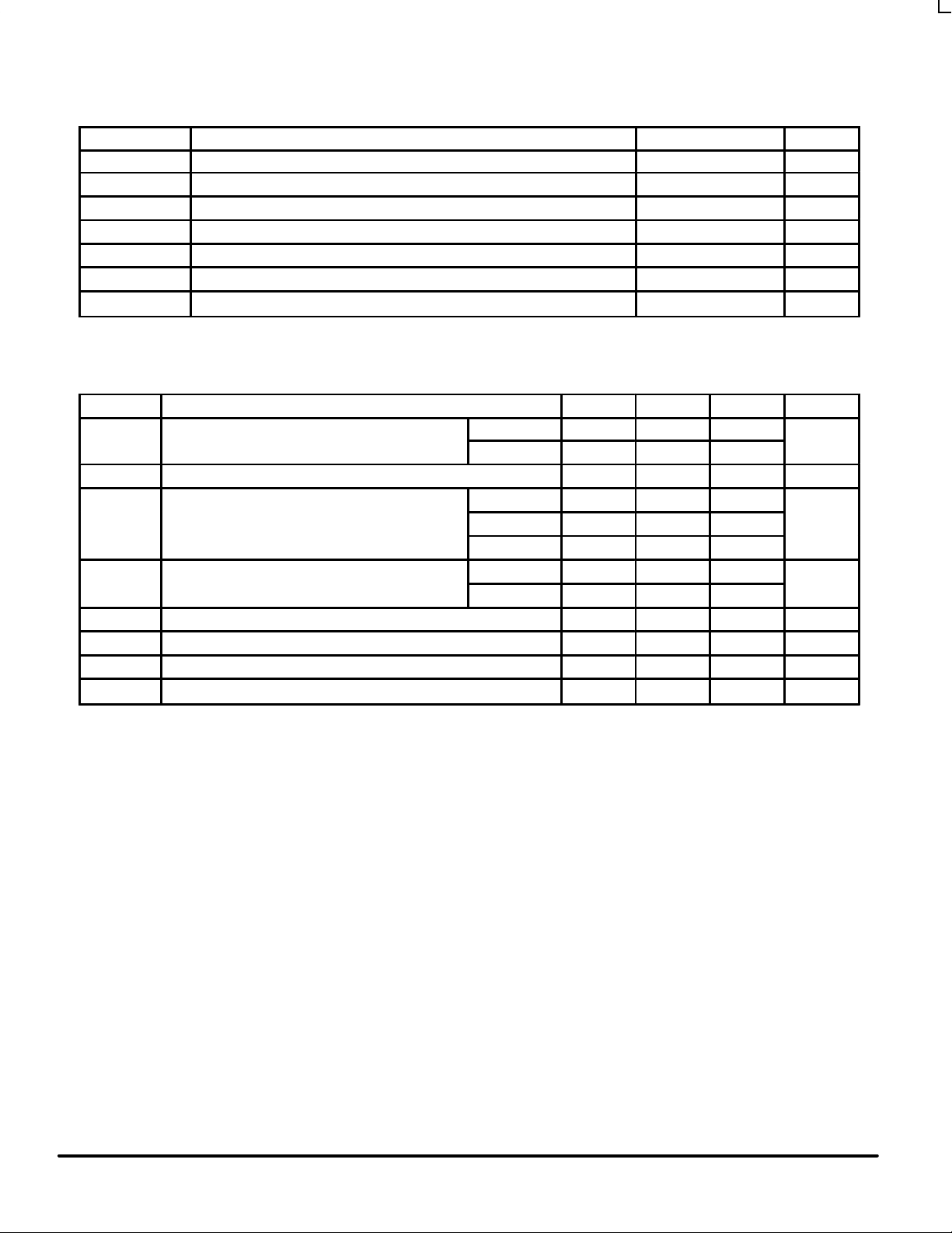
MAXIMUM RATINGS*
Symbol Parameter Value Unit
V
CC
DC Supply Voltage (Referenced to GND) –0.5 to +7.0 V
V
in
DC Input Voltage (Referenced to GND) –0.5 to VCC +0.5 V
V
out
DC Output Voltage (Referenced to GND) –0.5 to VCC +0.5 V
I
in
DC Input Current, per Pin ±20 mA
I
out
DC Output Sink/Source Current, per Pin ±50 mA
I
CC
DC VCC or GND Current per Output Pin ±50 mA
T
stg
Storage Temperature –65 to +150 °C
* Maximum Ratings are those values beyond which damage to the device may occur. Functional operation should be restricted to the Recommended
Operating Conditions.
RECOMMENDED OPERATING CONDITIONS
Symbol Parameter Min Typ Max Unit
′AC 2.0 5.0 6.0
VCCSupply Voltage
′ACT 4.5 5.0 5.5
V
Vin, V
out
DC Input Voltage, Output Voltage (Ref. to GND) 0 V
CC
V
VCC @ 3.0 V 150
Input Rise and Fall Time (Note 1)
′AC Devices except Schmitt Inputs
VCC @ 4.5 V 40 ns/V
r
, t
f
′AC Devices except Schmitt Inputs
VCC @ 5.5 V 25
VCC @ 4.5 V 10
tr, t
f
Input Rise and Fall Time (Note 2)
′ACT Devices except Schmitt Inputs
VCC @ 5.5 V 8.0
ns/V
T
J
Junction Temperature (PDIP) 140 °C
T
A
Operating Ambient Temperature Range –40 25 85 °C
I
OH
Output Current — High –24 mA
I
OL
Output Current — Low 24 mA
1. Vin from 30% to 70% VCC; see individual Data Sheets for devices that differ from the typical input rise and fall times.
2. Vin from 0.8 V to 2.0 V; see individual Data Sheets for devices that differ from the typical input rise and fall times.
tr, t
f
Input Rise and Fall Time (Note 2)
 Loading...